
Data Sheet
%
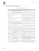
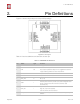
2. Pin Definitions
9
MTMS
I/O
GPIO 14; HSPI_CLK
10
MTDI
I/O
GPIO 12; HSPI_MISO
11
VDDPST
P
Digital/IO Power Supply (1.8V ~ 3.3V)
12
MTCK
I/O
GPIO 13; HSPI_MOSI; UART0_CTS
13
MTDO
I/O
GPIO 15; HSPI_CS; UART0_RTS
14
GPIO2
I/O
UART Tx during flash programming; GPIO2
15
GPIO0
I/O
GPIO0; SPI_CS2
16
GPIO4
I/O
GPIO 4
17
VDDPST
P
Digital/IO Power Supply (1.8V ~ 3.3V)
18
SDIO_DATA_2
I/O
Connect to SD_D2 (Series R: 200Ω); SPIHD; HSPIHD; GPIO 9
19
SDIO_DATA_3
I/O
Connect to SD_D3 (Series R: 200Ω); SPIWP; HSPIWP; GPIO 10
20
SDIO_CMD
I/O
Connect to SD_CMD (Series R: 200Ω); SPI_CS0; GPIO 11
21
SDIO_CLK
I/O
Connect to SD_CLK (Series R: 200Ω); SPI_CLK; GPIO 6
22
SDIO_DATA_0
I/O
Connect to SD_D0 (Series R: 200Ω); SPI_MSIO; GPIO 7
23
SDIO_DATA_1
I/O
Connect to SD_D1 (Series R: 200Ω); SPI_MOSI; GPIO 8
24
GPIO5
I/O
GPIO 5
25
U0RXD
I/O
UART Rx during flash programming; GPIO 3
26
U0TXD
I/O
UART Tx during flash progamming; GPIO 1; SPI_CS1
27
XTAL_OUT
I/O
Connect to crystal oscillator output, can be used to provide BT
clock input
28
XTAL_IN
I/O
Connect to crystal oscillator input
29
VDDD
P
Analog Power 2.5V ~ 3.6V
30
VDDA
P
Analog Power 2.5V ~ 3.6V
31
RES12K
I
Serial connection with a 12 kΩ resistor and connect to the
ground
32
EXT_RSTB
I
External reset signal (Low voltage level: Active)
Pin
Name
Type
Function
📖 Note:
GPIO2, GPIO0, and MTDO are configurable on PCB as the 3-bit strapping register that determines the
booting mode and the SDIO timing mode.
Espressif
% /%6 25
2017.04