ESP8266EX Datasheet Version 5.
About This Guide This document introduces the specifications of ESP8266EX, including the following topics. Chapter Title Subject Chapter 1 Overview Provides an overview of ESP8266, including its features, protocols, technical parameters and applications. Chapter 2 Pin Definitions Provides the pin layout and the relevant description.
Table of Contents 1. Overview ................................................................................................................................ 1 1.1. Wi-Fi Protocols ...........................................................................................................................1 1.2. Main Technical Specifications ....................................................................................................3 1.3. Applications ..................................................
5. Electrical Specifications ......................................................................................................19 5.1. Electrical Characteristics ..........................................................................................................19 5.2. Power Consumption ................................................................................................................19 5.3. Wi-Fi Radio Characteristics ..................................................................
1. Overview % 1. Overview Espressif’s ESP8266EX delivers highly integrated Wi-Fi SoC solution to meet users’ continuous demands for efficient power usage, compact design and reliable performance in the Internet of Things industry. With the complete and self-contained Wi-Fi networking capabilities, ESP8266EX can perform either as a standalone application or as the slave to a host MCU. When ESP8266EX hosts the application, it promptly boots up from the flash.
1. Overview % • WMM power low U-APSD. • Multiple queue management to fully utilize traffic prioritization defined by 802.11e standard. • UMA compliant and certified. • 802.1h/RFC1042 frame encapsulation. • Scattered DMA for optimal CPU off load on Zero Copy data transfer operations. • Antenna diversity and selection (software managed hardware). • Clock/power gating combined with 802.11-compliant power management dynamically adapted to current connection condition providing minimal power consumption.
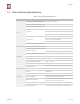
1. Overview % 1.2. Main Technical Specifications Table 1-1. Main Technical Specifications Categories Items Parameters Standards FCC/CE/TELEC/SRRC Protocols 802.11 b/g/n/e/i Frequency Range 2.4G ~ 2.5G (2400M ~ 2483.5M) 802.11 b: +20 dBm Wi-Fi Tx Power 802.11 g: +17 dBm 802.11 n: +14 dBm 802.11 b: -91 dbm (11 Mbps) Rx Sensitivity 802.11 g: -75 dbm (54 Mbps) 802.
1. Overview % 1.3. Applications Espressif • Home Appliances • IP Cameras • Home Automation • Sensor Networks • Smart Plugs and Lights • Wearable Electronics • Mesh Network • Wi-Fi Location-aware Devices • Industrial Wireless Control • Security ID Tags • Baby Monitors • Wi-Fi Position System Beacons % /%25 4 2017.
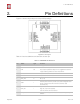
2. Pin Definitions % 2. Pin Definitions Figure 2-1 shows the pin layout for 32-pin QFN package. ! Figure 2-1. Pin Layout Table 2-1 lists the definitions and functions of each pin. Table 2-1. ESP8266EX Pin Definitions Pin Name Type Function 1 VDDA P Analog Power 2.5V ~ 3.6V 2 LNA I/O Chip output impedance=39+j6 Ω. It is suggested to retain the π-type matching network to match the antenna. 3 VDD3P3 P Amplifier Power 2.5V ~ 3.6V 4 VDD3P3 P Amplifier Power 2.5V ~ 3.
2. Pin Definitions % Pin Name Type Function 9 MTMS I/O GPIO 14; HSPI_CLK 10 MTDI I/O GPIO 12; HSPI_MISO 11 VDDPST P Digital/IO Power Supply (1.8V ~ 3.3V) 12 MTCK I/O GPIO 13; HSPI_MOSI; UART0_CTS 13 MTDO I/O GPIO 15; HSPI_CS; UART0_RTS 14 GPIO2 I/O UART Tx during flash programming; GPIO2 15 GPIO0 I/O GPIO0; SPI_CS2 16 GPIO4 I/O GPIO 4 17 VDDPST P Digital/IO Power Supply (1.8V ~ 3.
3. Functional Description % 3. Functional Description The functional diagram of ESP8266EX is shown as in Figure 3-1. RF receive MAC Analog receive PMU Analog transmit VCO 1/2 Crystal Digital baseband RF transmit PLL UART GPIO Switch RF balun Registers Interface I2C I2S Sequencers SDIO PWM Accelerator PLL Bias circuits CPU ADC SPI SRAM PMU Flash % Figure 3-1. Functional Block Diagram 3.1. CPU, Memory, and Flash 3.1.1.
3. Functional Description % • RAM size < 50 kB, that is, when ESP8266EX is working under the Station mode and connects to the router, programmable space accessible in heap + data section is around 50 kB. • There is no programmable ROM in the SoC, therefore, user program must be stored in an external SPI flash. 3.1.3. External Flash ESP8266EX uses external SPI flash to store user programs, and supports up to 16 MB memory capacity theoretically. The minimum flash memory of ESP8266EX is shown in Table 3-1.
3. Functional Description % Table 3-2. High Frequency Clock Specifications Parameter Symbol Min Max Unit Frequency FXO 24 52 MHz Loading capacitance CL - 32 pF Motional capacitance CM 2 5 pF Series resistance RS 0 65 Ω Frequency tolerance ΔFXO -15 15 ppm Frequency vs temperature (-25°C ~ 75°C) ΔFXO,Temp -15 15 ppm 3.3.2. External Clock Requirements An externally generated clock is available with the frequency ranging from 24 MHz to 52 MHz.
3. Functional Description % Table 3-4. Frequency Channel Channel No. Frequency (MHz) Channel No. Frequency (MHz) 1 2412 8 2447 2 2417 9 2452 3 2422 10 2457 4 2427 11 2462 5 2432 12 2467 6 2437 13 2472 7 2442 14 2484 3.4.2. 2.4 GHz Receiver The 2.4 GHz receiver down-converts the RF signals to quadrature baseband signals and converts them to the digital domain with 2 high resolution high speed ADCs.
3. Functional Description % 3.5. Wi-Fi ESP8266EX implements TCP/IP, the full 802.11 b/g/n/e/i WLAN MAC protocol and Wi-Fi Direct specification. It supports not only basic service set (BSS) operations under the distributed control function (DCF) but also P2P group operation compliant with the latest Wi-Fi P2P protocol. Low level protocol functions are handled automatically by ESP8266EX. • RTS/CTS • acknowledgement • fragmentation and defragmentation • aggregation • frame encapsulation (802.
3. Functional Description % CHIP_PU CHIP_PU Off Sleep Criteria Sleep Criteria Deep Sleep Sleep XTAL Off WAKEUP Events Wakeup XTAL_SETTLE CPU On Work Tx Rx ! Figure 3-2. Power Management • Off: CHIP_PU pin is low. The RTC is disabled. All registers are cleared. • Deep-sleep: Only RTC is powered on – the rest of the chip is powered off. Recovery memory of RTC can save basic Wi-Fi connection information. • Sleep: Only the RTC is operating. The crystal oscillator is disabled.
4. Peripheral Interface % 4. Peripheral Interface 4.1. General Purpose Input/Output Interface (GPIO) ESP8266EX has 17 GPIO pins which can be assigned to various functions by programming the appropriate registers. Each GPIO can be configured with internal pull-up or pull-down, or set to high impedance, and when configured as an input, the data are stored in software registers; the input can also be set to edge-trigger or level trigger CPU interrupts.
4. Peripheral Interface % 4.3. Serial Peripheral Interface (SPI/HSPI) ESP8266EX has 3 SPIs. • One general Slave/Master SPI • One Slave SDIO/SPI • One general Slave/Master HSPI Functions of all these pins can be implemented via hardware. The pin definitions are described as below. 4.3.1. General SPI (Master/Slave) Table 4-2.
4. Peripheral Interface % Table 4-4. Pin Definitions of I2C Pin Name Pin Num IO Function Name MTMS 9 IO14 I2C_SCL GPIO2 14 IO2 I2C_SDA Both I2C Master and I2C Slave are supported. I2C interface functionality can be realized via software programming, and the clock frequency is 100 kHz at a maximum. It should be noted that I2C clock frequency should be higher than the slowest clock frequency of the slave device. 4.5.
4. Peripheral Interface % Pin Type UART1 Pin Name Pin Num IO Function Name MTCK 12 IO13 U0CTS GPIO2 14 IO2 U1TXD SD_D1 23 IO8 U1RXD Data transfers to/from UART interfaces can be implemented via hardware. The data transmission speed via UART interfaces reaches 115200 x 40 (4.5 Mbps). UART0 can be used for communication. It supports fluid control. Since UART1 features only data transmit signal (Tx), it is usually used for printing log.
4. Peripheral Interface % Table 4-8. Pin Definitions of IR Remote Control Pin Name Pin Num IO Function Name MTMS 9 IO14 IR Tx GPIO5 24 IO 5 IR Rx The functionality of Infrared remote control interface can be implemented via software programming. NEC coding, modulation, and demodulation are used by this interface. The frequency of modulated carrier signal is 38 kHz, while the duty ratio of the square wave is 1/3.
4. Peripheral Interface % RF Calibration Process Optimize the RF circuit conditions based on the value of vdd33_const. The permissible error is ±0.2V. User Programming Use system_adc_read instead of system_get_vdd33. 📖 Notes: esp_init_data_default.bin is provided in SDK package which contains RF initialization parameters (0 ~ 127 bytes). You can define the 107th byte in esp_init_data_default.bin to vdd33_const as below.
5. Electrical Specifications % 5. Electrical Specifications 5.1. Electrical Characteristics Table 5-1. Electrical Characteristics Parameters Conditions Min Typical Max Unit Storage Temperature Range - -40 Normal 125 ℃ Maximum Soldering Temperature IPC/JEDEC JSTD-020 - - 260 ℃ Working Voltage Value - 2.5 3.3 3.6 V VIL/VIH - -0.3/0.75VIO - 0.25VIO/3.6 VOL/VOH - N/0.8VIO - 0.
5. Electrical Specifications % 📖 Notes: ① Modem-sleep mode is used in the applications that require the CPU to be working, as in PWM or ② I2S applications. According to 802.11 standards (like U-APSD), it shuts down the Wi-Fi Modem circuit while maintaining a Wi-Fi connection with no data transmission to optimize power consumption. E.g. in DTIM3, maintaining a sleep of 300 ms with a wakeup of 3 ms cycle to receive AP’s Beacon packages at interval requires about 15 mA current.
6. Package Information % 6. Package Information ! Figure 6-1. ESP8266EX Package Espressif % /% 25 21 2017.
Appendix Ⅰ % I. Appendix - Pin List For detailed pin information, please see ESP8266 Pin List. • Digital Die Pin List • Buffer Sheet • Register List • Strapping List 📖 Notes: • INST_NAME refers to the IO_MUX REGISTER defined in eagle_soc.h, for example MTDI_U refers to PERIPHS_IO_MUX_MTDI_U. • Net Name refers to the pin name in schematic. • Function refers to the multifunction of each pin pad. • Function number 1 ~ 5 correspond to FUNCTION 0 ~ 4 in SDK.
Appendix Ⅱ % II. Appendix - Learning Resources II.1. Must-Read Documents • ESP8266 Quick Start Guide Description: This document is a quick user guide to getting started with ESP8266. It includes an introduction to the ESP-LAUNCHER, instructions on how to download firmware to the board and run it, how to compile the AT application, as well as the structure and debugging method of RTOS SDK. Basic documentation and other related resources for the ESP8266 are also provided.
Appendix Ⅱ % Description: This webpage provides links both to the latest version of the ESP8266 SDK and the older ones. • ESP8266 Tools Description: This webpage provides links to both the ESP8266 flash download tools and the ESP8266 performance evaluation tools. • ESP8266 APK • ESP8266 Certification and Test Guide • ESP8266 BBS • ESP8266 Resources Espressif % /% 25 24 2017.
Disclaimer and Copyright Notice Information in this document, including URL references, is subject to change without notice. THIS DOCUMENT IS PROVIDED AS IS WITH NO WARRANTIES WHATSOEVER, INCLUDING ANY WARRANTY OF MERCHANTABILITY, NON-INFRINGEMENT, FITNESS FOR ANY PARTICULAR PURPOSE, OR ANY WARRANTY OTHERWISE ARISING OUT OF ANY PROPOSAL, SPECIFICATION OR SAMPLE. All liability, including liability for infringement of any proprietary rights, relating to use of information in this document is disclaimed.