CPMC-1553R User’s Guide
CPMC-1553R User’s Guide CA.DT.
Corporate Headquarters 150, rue Marcellin Berthelot ZI Toulon-Est BP 244 83078 TOULON Cedex 9 France Tel : +33 - (0) 4 94 16 34 00 Fax : +33 - (0) 4 94 16 34 01 USA Headquarters 1203 New Hope Road Raleigh - NC 27610 USA Tel : +1 - (800) 848 2330 Tel : +1 - (919) 231 8000 Fax : +1 - (919) 231 8001 International Sales Department 67, rue du Charles De-Gaulle 78350 JOUY-EN-JOSAS France Tel : +33 - (0) 1 39 56 72 72 Fax : +33 - (0) 1 39 56 72 70 United Kingdom Cornwell Business Park 31 Salthouse Road Brackmil
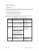
Table of Contents Chapter 1 1.1 1.2 1.3 1.4 Introduction................................................................................................................................ 1-1 Manual Overview....................................................................................................................... 1-1 CPMC-1553R Features .............................................................................................................. 1-2 CPMC-1553R Options..............................
Chapter 1 − Introduction 1.1 Manual Overview This manual describes the CPMC-1553R board from Thales Computers. Chapter 1 summarizes the board’s features and provides installation instructions. Chapter 2 describes its functional characteristics. Appendix A is a list of the abbreviations used in this manual. This manual uses the following terminology conventions: • Addresses and signal names are shown in capital letters. • An asterisk* after a signal name indicates active low.
1.2 CPMC-1553R Features The CPMC-1553R is a single, conduction-cooled, PMC card with two dual-redundant MIL-STD-1553 Buses.
1.3 CPMC-1553R Options Figure 2 shows the standard options available for the CPMC-1553R. CPMC-1553R-__ Environment Industrial/-SA ................................................................................. I Rugged/-RA.................................................................................... R Militarized/-RC .............................................................................. M __ Channels 1 Channel................................................................
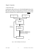
Chapter 2 − Operation 2.1 Functional Description The CPMC-1553R is a PMC card with one or two, dual-redundant MIL-STD-1553B buses, eight user inputs, and eight user outputs. The board interfaces to the user I/O through the PMC connector Pn4. Two PMC connectors, Pn1 and Pn2 provide a direct connection to the PCI Bus. The Altera FLEX10 Programmable Logic Device (PLD) and the ILC-DDC Mini-ACE Device provide the interface between the PCI bus and the MIL-STD-1553B bus.
2.2 PCI Bus Interface An Altera FLEX10 PLD provides the interface between the PCI Bus and the ILC-DDC Mini-ACE device. The FLEX10 operates at 33MHz, is powered by 5V or 3.3V, has a 32-bit data path, and is compliant with the PCI Local Bus Specification, Revision 2.1. The CPMC-1553R is a target on the PCI Bus. 2.2.1 PCI Configuration Space The PCI configuration space consists of a block of 64 configuration DWORDS, of which, the first 16 are defined by the PCI Special Interest Group (PCI SIG).
Table 3.
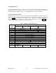
2.2.1.4 Status Register The Status Register is a 16-bit read/write register that provides the status of busrelated events. Read transactions tell you the current status of the bits. The Status Register is cleared by writing a logic one to that bit. Writing a logic zero has no affect on the registers. The status register is defined in Table 5. The default value of the status register is 0x0400. Data Bit 8..0 10..9 11 12 13 14 15 Table 5.
2.2.1.8 Latency Timer Register The Latency Timer register is not supported. 2.2.1.9 Header Type Register The Header Type register is an 8-bit, read-only register that identifies the CPMC-1553R board as a single function device. This register returns a value of 0x00 when read. 2.2.1.10 Built-In Self Test Register The Built-In Self Test (BIST) Register is not supported. 2.2.1.11 Base Address Registers Each of the six Base Address Registers (BAR#) has identical attributes.
2.2.1.15 Expansion ROM Base Address Register supported. The Expansion ROM Base Address Register is not 2.2.1.16 Interrupt Line Register The Interrupt Line Register is an 8-bit, read/write register that defines which system interrupt request line (on the system interrupt controller) the INTA* output is routed. The default value for this register is 0x00. 2.2.1.
PCI Address (AD15..AD0) 0000 0002 0004 0006 Table 7. Mapping of PCI Memory Space to ACE Internal Registers ACE Address Read/Write Description (ADDR15..
Table 7. Mapping of PCI Memory Space to ACE Internal Registers - Continued PCI Address ACE Address Read/Write Description (AD15..AD0) (ADDR15..
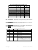
2.2.2.2 ACE Configuration and User I/O Register The ACE configuration used on the board can be read via PCI I/O space defined in BAR1, with an address offset of 0x0800. In addition, this register also provides the means for software to read the eight input bits and control the eight, open-drain output bits. The output bits are pulled to 5V using 4.7K ohm resistors. This register is defined in Table 8. Data Bit 31..24 23..16 15..12 11 10..8 7..3 2 1..0 Table 8.
2.2.2.4 ACE Reset Register This read/write register is accessible at 0x0808, BAR 1. Only bit 0 is used. After a PCI reset the register reads 0x00000001. To generate a reset to both ACE chips write a 0 to bit 0. A 0 holds both ACEs in reset. Write a 1 to bit D0 to unreset both ACEs. This register is provided only for test purposes and is not intended to be used as part of the normal CPMC-1553R operation. 2.2.2.5 ACE Memory Space The ACE memory space is mapped into the PCI memory space.
2.2.3 PCI I/O Space The PCI I/O space is not utilized by the CPMC-1553R board. 2.2.4 Interrupt A (INTA*) The CPMC-1553R board generates INTA* on the PCI Bus when either of the Mini-ACE devices generates an interrupt or an interrupt occurs from one of the user-defined input lines. The interrupt conditions are configurable through software. 2.3 MIL-STD-1553B Bus Each MIL-STD-1553B bus is implemented using an ILC-DDC Mini-ACE device with 64kB x 16 of shared RAM.
Pin 1 3 5 7 9 11 13 15 17 19 21 23 25 27 29 31 33 35 37 39 41 43 45 47 49 51 53 55 57 59 61 63 Thales Computers Table 11.
2.4 Power Requirements The CPMC-1553R uses 3.3 volts and 5 volts power. VIO, +12 volts, and –12 volts are not used. The 3.3 volt supply powers the PCI interface and the 5 volt supply powers each of the ACEs. Typical current draw is at 25°C at the “Typical” power voltages. The “Maximum” current draw is over the worse case condition of voltage and temperature. Table 12 shows the power specifications for the board. Note that I5V0 is for each ACE installed. With two ACE chips installed double I5V0.
Appendix A − List of Abbreviations ACE BAR BC BIST BIT CIS MT IEEE I/O PCI PCI SIG PLD PMC RAM ROM RT TTL Advanced Communication Engine Base Address Register Bus Controller Built-In Self-Test Register Built-In-Test Card Information Structure Monitor Terminal Institute of Electrical and Electronic Engineers Input/Output Peripheral Component Interconnect PCI Special Interest Group Programmable Logic Device PCI Mezzanine Card Random Access Memory Read Only Memory Remote Terminal Transistor-Transistor Logic T
Vos remarques sur ce document / Your comments on this document Titre / Title: CPMC-1553R User’s Guide No de référence / Reference No: CA.DT.356-0e ID production / Product ID: 9903 ERREURS DETECTEES / ERRORS FOUND IN THIS DOCUMENT AMELIORATIONS SUGGEREES / SUGGESTIONS FOR IMPROVEMENT TO THIS DOCUMENT ■ Vos remarques et suggestions seront attentivement examinées. Si vous désirez une réponse écrite, veuillez indiquer votre adresse postale complète.