
User manual

Hardware description
UM1900
6/15
DocID027905 Rev 1
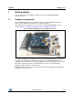
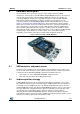
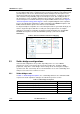
In this scenario, microphone acquisition functions thus: a precise clock signal is generated
by I²S peripheral while SPI is configured in slave mode and is fed by the same timing signal
generated by I²S. This clock is then halved by a timer and input to the microphones: the
SPI and I²S peripherals operate at twice the microphone frequency, so that they can read
data on both the rising and falling edge of the microphone clock, thus reading the bits of
two microphones each. A software demuxing step is required to separate the signal from
the two microphones and allows further processing like PDM to PCM conversion. Figure 4:
"General acquisition strategy block diagram" shows a simplified diagram of the acquisition
process described in this paragraph. For further information about MEMS microphone and
PDM to PCM decimation, please refer www.st.com and AN3998.
For single microphone acquisition, the correct microphone timer is generated directly by I²S
and one single microphone data line is read by the same peripheral. For an example
application of microphone acquisition, decimation and streaming based on X-NUCLEO-
CCA02M1 board, please refer the board firmware package (order code: X-CUBE-
MEMSMIC1).
Figure 4: General acquisition strategy block diagram
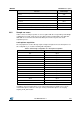
3.3 Solder bridges configurations
Various board configurations are possible, depending on the use cases. MEMS
microphones can be connected (or disconnected) to morpho pins, and thus to MCU
peripherals, using ad hoc solder bridges. Clock routing can als be changed according to
specific needs. This section helps the user understand the role of each solder bridge and
analyzes some of the more common use cases.
3.3.1 Solder bridges roles
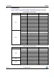
In Table 1: "Solder bridge descriptions", the solder bridge dunctions are summarized with
respect to the audio acquisition strategies described in the previous section.
Table 1: Solder bridge descriptions
Function
Solder bridge
Connects USB D- pin to OTG_FS_DM pin on the MCU
SB1
Connects USB D+ pin to OTG_FS_DP pin on the MCU
SB2
Routes onboard oscillator output to OSC_IN MCU pin
SB6
Connect microphone clock to MCU timer output channel
SB7
Routes I²S clock to SPI clock
SB8