
Datasheet


Table Of Contents
- 1 Absolute maximum ratings and operating conditions
- 2 Electrical characteristics
- 3 Typical characteristics
- Figure 2. Supply current (each amplifier) versus supply voltage
- Figure 3. Input bias current versus free air temperature
- Figure 4. High level output voltage versus high level output current
- Figure 5. High level output voltage versus high level output current
- Figure 6. Low level output voltage versus low level output current
- Figure 7. Low level output voltage versus low level output current
- Figure 8. Open-loop frequency response and phase shift
- Figure 9. Gain bandwidth product versus supply voltage
- Figure 10. Phase margin versus supply voltage
- Figure 11. Phase margin versus capacitive load
- Figure 12. Slew rate versus supply voltage
- Figure 13. Input voltage noise versus frequency
- 4 Package information
- 5 Ordering information
- 6 Revision history
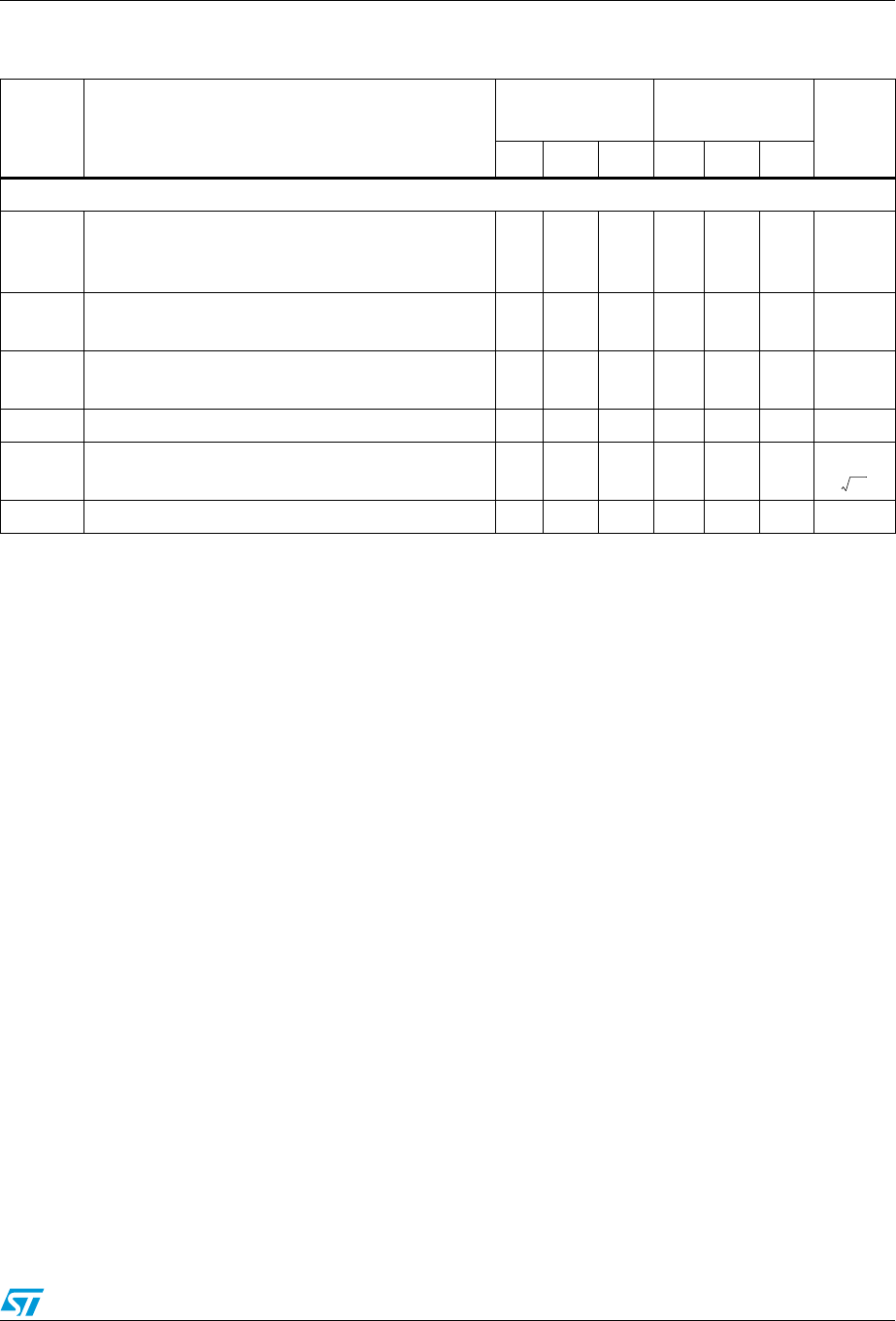
TS27M2, TS27M2A, TS27M2B Electrical characteristics
Doc ID 2306 Rev 2 5/14
AC performance
GBP
Gain bandwidth product
A
v
= 40 dB, R
L
= 100 kΩ, C
L
= 100 pF,
f
in
= 100 kHz
0.5 1 0.5 1 MHz
SR
Slew rate at unity gain
R
L
= 100 kΩ, C
L
= 100 pF, V
i
= 3 to 7 V
0.3 0.6 0.3 0.6 V/μs
φm
Phase margin at unity gain
A
v
= 40 dB, R
L
= 100 kΩ, C
L
= 100 pF
45 45 Degrees
K
OV
Overshoot factor 30 30 %
e
n
Equivalent input noise voltage
f = 1 kHz, R
s
= 100 Ω
38 38
V
o1
/V
o2
Channel separation 120 120 dB
1. Maximum values including unavoidable inaccuracies of industrial tests.
Table 3. Electrical characteristics at V
CC
+ = +10 V, V
CC
- = 0 V, T
amb
= +25° C
(unless otherwise specified) (continued)
Symbol Parameter
TS27M2xC
TS27M2xI
TS27M2xM
Unit
Min. Typ. Max. Min. Typ. Max.
nV
Hz
------------