
Datasheet


Table Of Contents
- 1 Absolute maximum ratings and operating conditions
- 2 Electrical characteristics
- 3 Typical characteristics
- Figure 2. Supply current (each amplifier) versus supply voltage
- Figure 3. Input bias current versus free air temperature
- Figure 4. High level output voltage versus high level output current
- Figure 5. High level output voltage versus high level output current
- Figure 6. Low level output voltage versus low level output current
- Figure 7. Low level output voltage versus low level output current
- Figure 8. Open-loop frequency response and phase shift
- Figure 9. Gain bandwidth product versus supply voltage
- Figure 10. Phase margin versus supply voltage
- Figure 11. Phase margin versus capacitive load
- Figure 12. Slew rate versus supply voltage
- Figure 13. Input voltage noise versus frequency
- 4 Package information
- 5 Ordering information
- 6 Revision history
August 2009 Doc ID 2306 Rev 2 1/14
14
TS27M2, TS27M2A, TS27M2B
Low-power CMOS dual operational amplifiers
Features
■ Wide supply voltage range: 3 to 16 V
■ Ultra-low consumption: 150 µA/op typ
■ Output voltage swing to ground
■ Excellent phase margin on capacitive load
■ Gain bandwidth product: 1 MHz typ
■ Vio down to 2 mV max. (B version)
Description
The TS27x2 series are low-cost and low-power
dual operational amplifiers designed to operate
with high-voltage single or dual supplies. These
operational amplifiers use the ST silicon gate
CMOS process, providing an excellent
consumption-speed ratio thanks to three different
power consumptions, making them ideal for low-
consumption applications:
I
CC
= 10 µA/amp: TS27L2 (very low power),
I
CC
= 150 µA/amp: TS27M2 (low power) and
I
CC
= 1 mA/amp: TS272 (high speed)
The devices also offer a very high input
impedance and extremely low input currents.
Their main advantage compared to JFET devices
is the very low input current drift with temperature
(Figure 3).
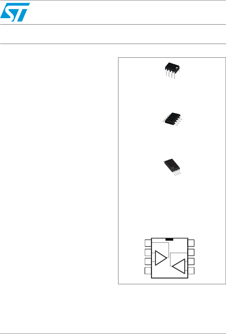
N
DIP8
(Plastic package)
D
SO-8
(Plastic micropackage)
P
TSSOP8
(Thin shrink small outline package)
Pin connections (top view)
In2+
V
CC-
1
2
3
5
4
8
7
6
In1+
In1-
Out2
+
_
Out1
In2-
+
_
V
CC+
In2+
V
CC-
1
2
3
5
4
8
7
6
In1+
In1-
Out2
+
_
Out1
In2-
+
_
V
CC+
www.st.com