
Datasheet
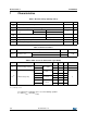
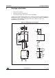
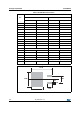
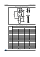
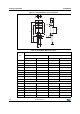
Table Of Contents
- Table 1. Device summary
- 1 Characteristics
- Table 2. Absolute ratings (limiting values)
- Table 3. Thermal resistance
- Table 4. Static electrical characteristics (per diode)
- Figure 1. Average forward power dissipation versus average forward current
- Figure 2. Normalized avalanche power derating versus pulse duration
- Figure 3. Average forward current versus ambient temperature, d = 0.5, (TO-220AC, D2PAK)
- Figure 4. Average forward current versus ambient temperature, d = 0.5, (TO-220FPAC)
- Figure 5. Non repetitive surge peak forward current versus overload duration - maximum values, per diode (TO-220AC, D2PAK)
- Figure 6. Non repetitive surge peak forward current versus overload duration - maximum values (TO-220FPAC)
- Figure 7. Relative variation of thermal impedance junction to case versus pulse duration (TO-220AC, D2PAK)
- Figure 8. Relative variation of thermal impedance junction to case versus pulse duration (TO-220FPAC)
- Figure 9. Reverse leakage current versus reverse voltage applied (typical values)
- Figure 10. Junction capacitance versus reverse voltage applied (typical values)
- Figure 11. Forward voltage drop versus forward current (maximum values)
- Figure 12. Thermal resistance junction to ambient versus copper surface under tab (D²PAK)
- 2 Package Information
- 3 Ordering Information
- 4 Revision history
Characteristics STPS8H100
4/10 DocID5387 Rev 11
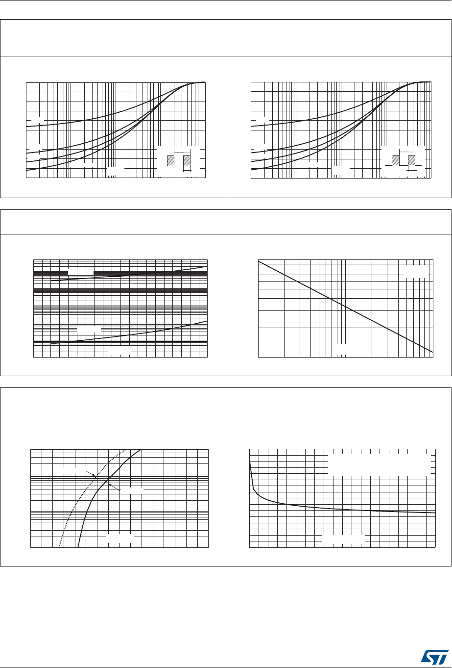
Figure 7. Relative variation of thermal
impedance junction to case versus pulse
duration (TO-220AC, D
2
PAK)
Figure 8. Relative variation of thermal
impedance junction to case versus pulse
duration (TO-220FPAC)
1E-4 1E-3 1E-2 1E-1 1E+0
0.0
0.2
0.4
0.6
0.8
1.0
t
p
(s)
Z
th(j-c)
/R
th(j-c)
δ = 0.1
δ = 0.2
δ = 0.5
Single pulse
T
δ
=t
p
/T=t
p
/T
t
p
t
p
1E-3 1E-2 1E-1 1E+0 1E+1
0.0
0.2
0.4
0.6
0.8
1.0
t
p
(s)
Z
th(j-c)
/R
th(j-c)
δ = 0.1
δ = 0.2
δ = 0.5
Single pulse
T
δ
=t
p
/T=t
p
/T
t
p
t
p
Figure 9. Reverse leakage current versus
reverse voltage applied (typical values)
Figure 10. Junction capacitance versus reverse
voltage applied (typical values)
0 102030405060708090100
1E-2
1E-1
1E+0
1E+1
1E+2
1E+3
5E+3
V
R
(V)
I
R
(µA)
T
j
=125°C
T
j
=25°C
1 10 100
100
200
500
1000
V
R
(V)
C(pF)
F=1MHz
T
j
=25°C
Figure 11. Forward voltage drop versus forward
current (maximum values)
Figure 12. Thermal resistance junction to
ambient versus copper surface under tab
(D²PAK)
0 0.2 0.4 0.6 0.8 1 1.2 1.4 1.6
0.1
1.0
10.0
50.0
V
FM
(V)
I
FM
(A)
T
j
=25°C
T
j
=125°C
0 4 8 12 16 20 24 28 32 36 40
0
10
20
30
40
50
60
70
80
S
(Cu)
(cm²)
R
th(j-a)
(°C/W)
Epoxy printed circuit board FR4,
copper thickness: 35 µm