
Datasheet


STP16CPP05 Summary description
Doc ID 15379 Rev 2 3/28
1 Summary description
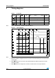
1.1 Pin connection and description
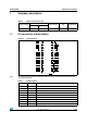
Figure 1. Pin connection
Note: The exposed pad should be electrically connected to a metal land electrically isolated or
connected to ground.
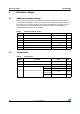
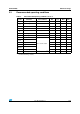
Table 2. Typical current accuracy
Output voltage
Current accuracy
Output current
V
DD
Temperature
Between bits Between ICs
≥ 1.3 V ± 1.2% ±5% ≥ 5 to 40 mA 3.3 V to 5 V 25 °C
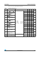
Table 3. Pin description
Pin N° Symbol Name and function
1 GND Ground terminal
2 SDI Serial data input terminal
3 CLK Clock input terminal
4 LE Latch input terminal
5-20 OUT 0-15 Output terminal
21 OE
Input terminal of output enable (active low)
22 SDO Serial data out terminal
23 R-EXT Input terminal of an external resistor for constant current programing
24 V
DD
Supply voltage terminal