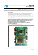
UM1018 User Manual STM32L152-EVAL evaluation board Introduction The STM32L152-EVAL evaluation board is a complete demonstration and development platform for STMicroelectronics’ ARM cortex-M3 core-based STM32L152VBT6 microcontroller supporting two I2C, two SPI and three USART channels, 12-bit ADC, 12-bit DAC, 16 KB internal SRAM and 128 KB Flash, USB FS, LCD controller, touch sensing and JTAG debugging support.
Contents UM01018 Contents 1 2 3 2/42 Features . . . . . . . . . . . . . . . . . . . . . . . . . . . . . . . . . . . . . . . . . . . . . . . . . . . 4 1.1 Demonstration software . . . . . . . . . . . . . . . . . . . . . . . . . . . . . . . . . . . . . . . 4 1.2 Order code . . . . . . . . . . . . . . . . . . . . . . . . . . . . . . . . . . . . . . . . . . . . . . . . . 4 Hardware and layout . . . . . . . . . . . . . . . . . . . . . . . . . . . . . . . . . . . . . . . . . 5 2.
UM01018 Contents 3.7 User USB Type B connector CN1 . . . . . . . . . . . . . . . . . . . . . . . . . . . . . . 23 3.8 Audio jack CN3 . . . . . . . . . . . . . . . . . . . . . . . . . . . . . . . . . . . . . . . . . . . . . 23 3.9 JTAG connector CN9 . . . . . . . . . . . . . . . . . . . . . . . . . . . . . . . . . . . . . . . . 24 3.10 Trace debugging connector CN8 . . . . . . . . . . . . . . . . . . . . . . . . . . . . . . . 24 3.11 MicroSD Card connector CN4 . . . . . . . . . . . . . . . . . . .
Features 1 UM01018 Features ● 1.1 Four 5 V power supply options: – Power jack – ST-LINK/V2 USB connector – User USB connector – Daughterboard ● Audio speaker and microphone connected to DAC and ADC of STM32L152VBT6 ● 2 GByte or more SPI interface MicroSD CardTM ● I2C compatible serial interface temperature sensor ● RS-232 communication ● IrDA transceiver ● JTAG and trace debug support, ST-LINK/V2 embedded.
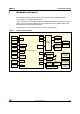
UM01018 2 Hardware and layout Hardware and layout The STM32L152-EVAL evaluation board is designed around the STM32L152VBT6 microcontroller in a 100-pin TQFP package. Figure 1 illustrates the connections between the STM32L152VBT6 and its peripherals (color LCD, touch sensing button, USB FS connector, temperature sensor, USART, IrDA, audio, MicroSD Card and embedded ST-LINK/V2). Figure 2 helps you to locate these features on the evaluation board. Figure 1.
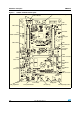
Hardware and layout Figure 2. UM01018 STM32L152-EVAL board layout ) % ! . ! #$ % ! 5# % " ). # 2 / $ % + 6 2 / & ' ( - $ 5 ! 1 % - , - 8%* 43) ! . ! * " ! # % " 8%* 43) % # . ) ) 7 2 , 6/42 $ )# + , !#1 2 0 / % . / 0 Doc ID 18141 Rev 2 .
UM01018 2.1 Hardware and layout Development and debug support Version 2 of the ST-LINK, called ST-LINK/V2, is embedded on the board. This tool allows on-board program loading and debugging of the STM32L using the JTAG or SWD interface. Third-party debug tools are also supported by the JTAG (CN9) or Trace (CN8) connectors. To communicate with the embedded ST-LINK/V2, a specific driver needs to be installed on your PC.
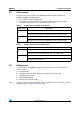
Hardware and layout Table 1. UM01018 Power related jumpers Jumper JP12 (selects one of the four possible power supply resources) Description Jumper setting For power supply from jack (CN12) to the STM32L152-EVAL only, JP12 is set as shown. PSU Daughter board USB STLink/V2 For power supply from daughterboard connector (CN6) to STM32L152-EVAL only, JP12 is set as shown. PSU Daughter board USB STLink/V2 For power supply from USB (CN1) to STM32L152-EVAL only, JP12 is set as shown.
UM01018 2.3 Hardware and layout Clock source Two clock sources are available on the STM32L152-EVAL evaluation board for the STM32L152VBT6 and embedded RTC. ● X1, 32 KHz crystal for embedded RTC ● X2, 8 MHz crystal with socket for the STM32L152VBT6 microcontroller, it can be removed from the socket when an internal RC clock is used. Table 2. 32 KHz crystal X1 related solder bridges Solder bridge Description PC14 is connected to 32 KHz crystal when SB1 is open (default setting).
Hardware and layout 2.5 UM01018 Boot option The STM32L152-EVAL evaluation board is able to boot from: ● Embedded user Flash ● System memory with boot loader for ISP ● Embedded SRAM for debugging The boot option is configured by setting switch SW1 (BOOT0) and SW2 (BOOT1). BOOT0 can also be configured via RS-232 connector CN2. Table 4. Boot related switches Switch Boot from STM32L152-EVAL boot from embedded user Flash when SW1 is set as shown.
UM01018 2.7 Hardware and layout Audio The STM32L152-EVAL evaluation board supports both: ● The speaker which is connected to the DAC output of the STM32L152VBT6 through an audio amplifier. ● The microphone which is connected to the ADC input of the STM32L152VBT6 through a microphone amplifier. The speaker can be enabled or disabled by setting JP16, refer to Table 7 for details. Table 7. Audio related jumpers Jumper Description Speaker amplifier U27 is enabled when JP16 is open (default setting).
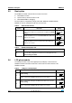
Hardware and layout Table 8. UM01018 RS-232 and IrDA related jumpers (continued) Jumper Description Setting USART2_CTS is connected to RS-232 transceiver when JP9 is set as shown (default setting). 1 2 3 Bootloader_RESET is connected to RS-232 transceiver when JP9 is set as shown. 1 2 3 JP9 JP7,JP8 Refer to Table 6 for USART3 settings. JP6 2.10 See Table 5 for Bootloader_BOOT0 settings.
UM01018 2.13 Hardware and layout Comparator Three I/Os are used to implement a comparator feature as shown in Figure 3. Figure 3. ● Comparator non-inverting input PB4 connected to LDR (R34). ● Comparator inverting input PB3 connected to potentiometer (RV3) used as variable threshold input for comparison to luminosity measured on LDR.
Hardware and layout Table 10. UM01018 Comparator and potentiometer related jumpers (continued) Jumper Description Setting PB5 is connected to I2C_SMB, the interrupt output of temperature sensor U18 when JP11 is closed (default setting). JP11 PB5 is disconnected from I2C_SMB but remains connected to COM_IN+ when JP11 is open for comparator application. 2.
UM01018 2.16 Hardware and layout IDD measurement The built-in IDD measurement circuit implemented allows the consumption measurement of the STM32L152C6T6 while the MCU is in Run or Low power saving modes. For IDD measurement the circuit below is implemented on STM32L152-EVAL. Figure 4.
Hardware and layout Figure 5. UM01018 STM32L152-EVAL IDD low power modes measurement timing diagram Wake-up period IDD measurement Wake-up event MCU mode Run Clear CNT event Stop or Standby 5 IDD_CNT_EN (PB15) Q12 = LOW_POWER_EN (T4 pin 3) Q13 = IDD_WAKEUP (PC13) Q13n = disconnect filter (U7 pin 4) 3 6 4 0 ms 150 ms 300 ms The principle used to measure a current when the STM32L is in Low power mode is: 1. Configure ADC to measure voltage on the IDD_Measurement pin (PA5). 2.
UM01018 2.16.3 Hardware and layout Ibias current measurement procedure In Low power mode the bias current of operational amplifier input (U10 pin 4) is not negligible compared to IDD current (typical Ibias is ~240 nA). To obtain a reliable MCU IDD measurement it is possible to subtract the bias current from the IDD low power measurement since this current is not sinked by the MCU. The procedure for accurate IDD measurement is: 1. Set jumper on JP4 pins 1 and 2. 2.
Connectors UM01018 3 Connectors 3.1 RS-232 connectors (CN2, CN5) Figure 6. RS-232 connector (viewed from front) -3 6 Table 13. RS-232 connector CN2 with HW flow control and ISP support Pin number Description Pin number 1 6 Bootloader_BOOT0 2 RS-232_RX (PD6) 7 RS-232_RTS(PD4) 3 RS-232_TX (PD5) 8 RS-232_CTS(PD3)/Bootloader_RESET 4 NC 9 NC 5 GND Table 14. RS-232 connector CN5 Pin number 3.
UM01018 3.3 Connectors Power connector (CN12) Your STM32L152-EVAL evaluation board can be powered from a DC 5 V power supply via the external power supply jack (CN12) shown in Figure 7. The central pin of CN12 must be positive. Figure 7. Power supply connector CN12 (viewed from front) $# 6 '.$ -3 6 3.4 Daughterboard extension connectors (CN6 and CN7) Two 50-pin male headers CN6 and CN7 can connect a daughterboard or standard wrapping board to the STM32L152-EVAL evaluation board.
Connectors UM01018 Table 15.
UM01018 Connectors Table 15. Daughterboard extension connector CN6 (continued) Pin Description Alternative function How to disconnect with function block on STM32L152-EVAL board 44 PE5 TRACE_D2 - 46 PB9 LCD glass_COM3 Remove LCD glass U20 48 +3V3 - - 50 GND - - Table 16.
Connectors UM01018 Table 16. Daughterboard extension connector CN7 (continued) Pin Description 3.
UM01018 3.6 Connectors ST-LINK/V2 USB type B connector CN11 The USB connector, CN11, is used to connect the embedded ST-LINK/V2 to the PC for board debugging. Figure 8. USB type B connector CN11 (viewed from front) -3 6 Table 17. USB type B connector CN11 Pin number 3.7 Description 1 VBUS (power) 2 DM 3 DP Pin number Description 4 GND 5,6 Shield User USB Type B connector CN1 Figure 9. USB type B connector CN1 (viewed from front) -3 6 Table 18.
Connectors 3.9 UM01018 JTAG connector CN9 Figure 10. JTAG debugging connector CN9 (viewed from above PCB) -3 6 Table 19. JTAG debugging connector CN9 Pin number 3.10 Description Pin number Description 1 3.3 V power 2 3.
UM01018 3.11 Connectors MicroSD Card connector CN4 Figure 11. MicroSD Card connector CN4 (viewed from front) -3 6 Table 21. MicroSD Card connector CN4 Pin number Description Pin number 1 5 MicroSDcard_CLK (PB13) 2 MicroSDcard_CS (PD7) 6 Vss/GND 3 MicroSDcard_DIN(PB15) 7 MicroSDcard_DOUT(PB14) 4 +3V3 8 9 3.12 Description MicroSDcard_detect (PE6) BNC connector CN13 Figure 12. Analog input connector CN13 (viewed from bottom) -3 6 Table 22.
Schematics 4 UM01018 Schematics The following schematics are listed.
UM01018 Figure 13. STM32L152-EVAL 1 2 3 U_MCU MCU.SchDoc U_LCD_Glass LCD_Glass.SCHDOC A SEG[0..43] COM[0..3] SEG[0..43] COM[0..3] Audio_IN Audio_OUT Audio_IN Audio_OUT U_Audio Audio.SchDoc U_Extension connector Extension connector.SCHDOC RESET# PH[0..2] PE[0..15] PD[0..15] PC[0..15] PB[0..15] PA[0..15] RESET# PH[0..2] PE[0..15] PD[0..15] PC[0..15] PB[0..15] PA[0..15] U_IDD_measurement IDD_measurement.
1 2 3 Schematics 28/42 Figure 14. MCU 4 PA[0..15] C28 6.8pF WAKEUP R43 2 10K 09.03290.
SEG40 SEG41 SEG36 SEG37 SEG32 SEG33 SEG28 SEG29 SEG20 SEG21 SEG11 SEG16 SEG4 SEG5 SEG0 SEG1 COM3 COM2 1 2 3 4 5 6 7 8 9 10 11 12 13 14 15 16 17 18 S28 S29 S24 S25 S20 S21 S16 S17 S12 S13 S8 S9 S4 S5 S0 S1 COM4 COM3 S31 S30 S27 S26 S23 S22 S19 S18 S15 S14 S11 S10 S7 S6 S3 S2 COM1 COM2 Doc ID 18141 Rev 2 1 B 36 35 34 33 32 31 30 29 28 27 26 25 24 23 22 21 20 19 SEG43 SEG42 SEG39 SEG38 SEG35 SEG34 SEG31 SEG30 SEG23 SEG22 SEG19 SEG18 SEG10 SEG6 SEG3 SEG2 COM0 COM1 UM01018 Figure 15.
1 2 3 Schematics 30/42 Figure 16.
UM01018 Figure 17. Peripherals 2 3 A BNC R45 PA5 R47 0 0 C31 [N/A] R48 0 JP14 LD3 Red 1 R131 SB5 R42 50 R123 2 PD1 R130 2 1 0 +3V3 +3V3 LED2 R9 1K R124 0 PD4 U1A TS3702IPT 2 +3V3 R122 0 PD5 R6 1K2 LED4 LEDs R5 1K BNC connector 5 B PB12 PB3 PB5 6 4 2 3 1 2 1 R120 5 3 1 LD6 Green TS3702IPT VDD>2.2V B2 WKUP C81 [N/A] JP17 Potentiometer COM_INCOM_IN+ R4 2K 100 RV3 210K 3 Doc ID 18141 Rev 2 R34 VT9ON1 6 R133 VDD VDD 4 8.
1 2 3 Schematics 32/42 Figure 18. Power 4 A A U26 ZEN056V130A24LS 1 1 3 2 Z1 SMAJ5.0A-TR 2 DC-10B C61 100nF SV SG CV 4 5 6 CG1 CG2 CG3 3 C58 220uF TP6 +3V3 U22 LD1086D2M33 +5V Vin C65 47uF +3V3 2 Vout 3 VDD 2 C55 10uF C51 100nF 1 JP13 BNX002-01 B TP7 VDD_ADJ U24 LD1086D2M +5V Vin Vout 2 R94 124[1%] VDD_ADJ ADJ 3 1 Power Supply VDD_ADJ [1.65V to 3.6V] R95 40.
UM01018 Figure 19.
1 2 3 Schematics 34/42 Figure 20.
UM01018 Figure 21.
1 2 3 Schematics 36/42 Figure 22.
UM01018 Figure 23. Temperature sensor 1 2 3 4 A A VDD 2 R67 R68 R73 4K7 4K7 4K7 +3V3 TR1 FDN327N G B R63 R66 4K7 4K7 U18 I2C_SDA I2C_SLK I2C_SMB PB7 PB6 PB5 R62 R69 R61 0 0 0 1 1 2 3 4 3 S D 2 Doc ID 18141 Rev 2 B G 1 S 3 D TR2 FDN327N SDA VDD SCL A0 OS/INT A1 GND A2 8 7 6 5 C41 100nF STLM75M2E Temperature sensor C C D D STMicroelectronics Title: STM32L152-EVAL TemperatureSensor 1 2 3 Rev: B.4(PCB.
1 2 +3V3 3 LED_STLINK U23 STM32F103C8T6 48 47 46 45 44 43 42 41 40 39 38 37 +3V3 X3 2 C54 20pF +3V3 8MHz +3V3 1 2 3 4 SWIM_PU_CTRL 5 OSC_IN OSC_OUT 6 STM_RST 7 8 C56 9 +3V3 100nF 10 AIN_1 11 12 R87 Red Yellow 36 35 34 33 32 31 30 29 28 27 26 25 VDD LD5 HSMF-A201-A00J1 R90 R85 4K7 4K7 AIN_1 R102 0 +3V3 VDD_2 VSS_2 JTMS PA12 PA11 PA10 PA9 PA8 S2_MOSI S2_MISO S2_CK PB12 A STM_JTMS_SWDIO USB_DP USB_DM T_SWO LED_STLINK +3V3 MCO B T_JTMS T_JTCK T_SWDIO_IN 13 14 15 16 17 18 19 20
UM01018 Figure 25.
1 2 3 Schematics 40/42 Figure 26.
UM01018 5 Revision history Revision history Table 23. Date Document revision history Revision Changes 13-Dec-2010 1 Initial release. 14-Nov-2011 2 Modified LED in Figure 17: Peripherals and updated schematics.
UM01018 Please Read Carefully: Information in this document is provided solely in connection with ST products. STMicroelectronics NV and its subsidiaries (“ST”) reserve the right to make changes, corrections, modifications or improvements, to this document, and the products and services described herein at any time, without notice. All ST products are sold pursuant to ST’s terms and conditions of sale.