
Datasheet

DocID022799 Rev 6 99/132
STM32L15xCC STM32L15xRC STM32L15xUC STM32L15xVC Electrical characteristics
111
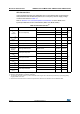
6.3.17 12-bit ADC characteristics
Unless otherwise specified, the parameters given in Table 56 are guaranteed by design.
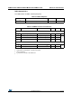
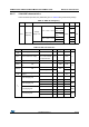
Table 55. ADC clock frequency
Symbol Parameter Conditions Min Max Unit
f
ADC
ADC clock
frequency
Voltage
range 1 & 2
2.4 V V
DDA
3.6 V
V
REF+ =
V
DDA
0.480
16
MHz
V
REF+
V
DDA
V
REF+
> 2.4 V
8
V
REF+
V
DDA
V
REF+
2.4 V
4
1.8 V V
DDA
2.4 V
V
REF+ =
V
DDA
8
V
REF+
V
DDA
4
Voltage range 3 4
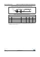
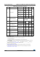
Table 56. ADC characteristics
Symbol Parameter Conditions Min Typ Max Unit
V
DDA
Power supply - 1.8 - 3.6
VV
REF+
Positive reference voltage
2.4 V V
DDA
3.6 V
V
REF+
must be below
or equal to V
DDA
1.8
(1)
-V
DDA
V
REF-
Negative reference voltage - - V
SSA
-
I
VDDA
Current on the V
DDA
input
pin
- - 1000 1450
µA
I
VREF
(2)
Current on the V
REF
input
pin
Peak -
400
700
Average - 450
V
AIN
Conversion voltage
range
(3)
-0
(4)
-V
REF+
V
f
S
12-bit sampling rate
Direct channels - - 1
Msps
Multiplexed channels - - 0.76
10-bit sampling rate
Direct channels - - 1.07
Msps
Multiplexed channels - - 0.8
8-bit sampling rate
Direct channels - - 1.23
Msps
Multiplexed channels - - 0.89
6-bit sampling rate
Direct channels - - 1.54
Msps
Multiplexed channels - - 1