
Datasheet

DocID022799 Rev 6 95/132
STM32L15xCC STM32L15xRC STM32L15xUC STM32L15xVC Electrical characteristics
111
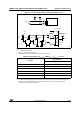
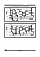
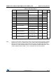
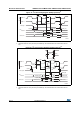
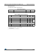
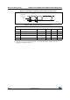
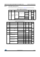
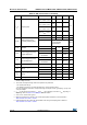
Note: Refer to the I2S section of the product reference manual for more details about the sampling
frequency (Fs), f
MCK
, f
CK
and D
CK
values. These values reflect only the digital peripheral
behavior, source clock precision might slightly change them. DCK depends mainly on the
ODD bit value, digital contribution leads to a min of (I2SDIV/(2*I2SDIV+ODD) and a max of
(I2SDIV+ODD)/(2*I2SDIV+ODD). Fs max is supported for each mode/condition.
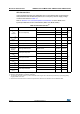
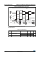
t
r(CK)
I2S clock rise time
Capacitive load CL=30pF -
8
ns
t
f(CK)
I2S clock fall time 8
t
v(WS)
WS valid time Master mode 4 24
t
h(WS)
WS hold time Master mode 0 -
t
su(WS)
WS setup time Slave mode 15 -
t
h(WS)
WS hold time Slave mode 0 -
t
su(SD_MR)
Data input setup time Master receiver 8 -
t
su(SD_SR)
Data input setup time Slave receiver 9 -
t
h(SD_MR)
Data input hold time
Master receiver 5 -
t
h(SD_SR)
Slave receiver 4 -
t
v(SD_ST)
Data output valid time
Slave transmitter
(after enable edge)
-64
t
h(SD_ST)
Data output hold time
Slave transmitter
(after enable edge)
22 -
t
v(SD_MT)
Data output valid time
Master transmitter
(after enable edge)
-12
t
h(SD_MT)
Data output hold time
Master transmitter
(after enable edge)
8-
1. The maximum for 256xFs is 8 MHz
Table 51. I2S characteristics
Symbol Parameter Conditions Min Max Unit