
Datasheet

Electrical characteristics STM32L15xCC STM32L15xRC STM32L15xUC STM32L15xVC
92/132 DocID022799 Rev 6
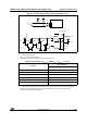
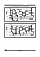
SPI characteristics
Unless otherwise specified, the parameters given in the following table are derived from
tests performed under ambient temperature, f
PCLKx
frequency and V
DD
supply voltage
conditions summarized in Table 14.
Refer to Section 6.3.12: I/O current injection characteristics for more details on the
input/output alternate function characteristics (NSS, SCK, MOSI, MISO).
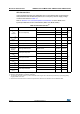
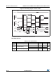
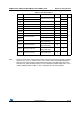
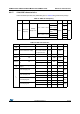
Table 50. SPI characteristics
(1)
Symbol Parameter Conditions Min Max
(2)
Unit
f
SCK
1/t
c(SCK)
SPI clock frequency
Master mode - 16
MHz
Slave mode - 16
Slave transmitter - 12
(3)
t
r(SCK)
(2)
t
f(SCK)
(2)
SPI clock rise and fall time Capacitive load: C = 30 pF - 6 ns
DuCy(SCK) SPI slave input clock duty cycle Slave mode 30 70 %
t
su(NSS)
NSS setup time Slave mode 4t
HCLK
-
ns
t
h(NSS)
NSS hold time Slave mode 2t
HCLK
-
t
w(SCKH)
(2)
t
w(SCKL)
(2)
SCK high and low time Master mode t
SCK
/25t
SCK
/2+3
t
su(MI)
(2)
Data input setup time
Master mode 5 -
t
su(SI)
(2)
Slave mode 6 -
t
h(MI)
(2)
Data input hold time
Master mode 5 -
t
h(SI)
(2)
Slave mode 5 -
t
a(SO)
(4)
Data output access time Slave mode 0 3t
HCLK
t
v(SO)
(2)
Data output valid time Slave mode - 33
t
v(MO)
(2)
Data output valid time Master mode - 6.5
t
h(SO)
(2)
Data output hold time
Slave mode 17 -
t
h(MO)
(2)
Master mode 0.5 -
1. The characteristics above are given for voltage range 1.
2. Based on characterization, not tested in production.
3. The maximum SPI clock frequency in slave transmitter mode is given for an SPI slave input clock duty cycle (DuCy(SCK))
ranging between 40 to 60%.
4. Min time is for the minimum time to drive the output and max time is for the maximum time to validate the data.