
Datasheet

DocID022799 Rev 6 89/132
STM32L15xCC STM32L15xRC STM32L15xUC STM32L15xVC Electrical characteristics
111
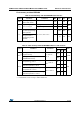
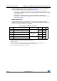
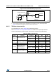
Figure 20. Recommended NRST pin protection
1. The reset network protects the device against parasitic resets.
2. The user must ensure that the level on the NRST pin can go below the V
IL(NRST)
max level specified in
Table 46. Otherwise the reset will not be taken into account by the device.
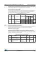
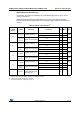
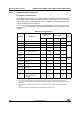
6.3.15 TIM timer characteristics
The parameters given in the Table 47 are guaranteed by design.
Refer to Section 6.3.13: I/O port characteristics for details on the input/output alternate
function characteristics (output compare, input capture, external clock, PWM output).
ai17854b
STM32L1xx
R
PU
NRST
(2)
V
DD
Filter
Internal reset
0.1 μF
External reset circuit(1)
Table 47. TIMx
(1)
characteristics
1. TIMx is used as a general term to refer to the TIM2, TIM3 and TIM4 timers.
Symbol Parameter Conditions Min Max Unit
t
res(TIM)
Timer resolution time
1-t
TIMxCLK
f
TIMxCLK
= 32 MHz 31.25 - ns
f
EXT
Timer external clock
frequency on CH1 to CH4
0f
TIMxCLK
/2 MHz
f
TIMxCLK
= 32 MHz 0 16 MHz
Res
TIM
Timer resolution - 16 bit
t
COUNTER
16-bit counter clock
period when internal clock
is selected (timer’s
prescaler disabled)
- 1 65536 t
TIMxCLK
f
TIMxCLK
= 32 MHz 0.0312 2048 µs
t
MAX_COUNT
Maximum possible count
- - 65536 × 65536 t
TIMxCLK
f
TIMxCLK
= 32 MHz - 134.2 s