
Datasheet

Electrical characteristics STM32L15xCC STM32L15xRC STM32L15xUC STM32L15xVC
88/132 DocID022799 Rev 6
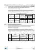
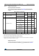
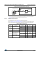
Figure 19. I/O AC characteristics definition
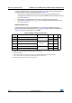
6.3.14 NRST pin characteristics
The NRST pin input driver uses CMOS technology. It is connected to a permanent pull-up
resistor, R
PU
(see Table 46)
Unless otherwise specified, the parameters given in Table 46 are derived from tests
performed under ambient temperature and V
DD
supply voltage conditions summarized in
Table 14.
ai14131c
10%
90%
50%
t
r(IO)out
OUTPUT
EXTERNAL
ON 50pF
Maximum frequency is achieved if (t
r
+ t
f
) ≤ 2/3)T and if the duty cycle is (45-55%)
10%
50%
90%
when loaded by 50pF
T
t
f(IO)out
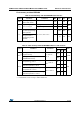
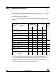
Table 46. NRST pin characteristics
Symbol Parameter Conditions Min Typ Max Unit
V
IL(NRST)
(1)
1. Guaranteed by design, not tested in production.
NRST input low level voltage - V
SS
-0.8
V
V
IH(NRST)
(1)
NRST input high level voltage - 1.4 - V
DD
V
OL(NRST)
(1)
NRST output low level
voltage
I
OL
= 2 mA
2.7 V < V
DD
< 3.6 V
--
0.4
I
OL
= 1.5 mA
1.65 V < V
DD
< 2.7 V
--
V
hys(NRST)
(1)
NRST Schmitt trigger voltage
hysteresis
--10%V
DD
(2)
2. 200 mV minimum value
-mV
R
PU
Weak pull-up equivalent
resistor
(3)
3. The pull-up is designed with a true resistance in series with a switchable PMOS. This PMOS contribution to
the series resistance is around 10%.
V
IN
V
SS
30 45 60 k
V
F(NRST)
(1)
NRST input filtered pulse - - - 50 ns
V
NF(NRST)
(1)
NRST input not filtered pulse - 350 - - ns