
Datasheet

Electrical characteristics STM32L15xCC STM32L15xRC STM32L15xUC STM32L15xVC
86/132 DocID022799 Rev 6
In the user application, the number of I/O pins which can drive current must be limited to
respect the absolute maximum rating specified in Section 6.2:
The sum of the currents sourced by all the I/Os on V
DD,
plus the maximum Run
consumption of the MCU sourced on V
DD,
cannot exceed the absolute maximum rating
I
VDD(x)
(see Table 12).
The sum of the currents sunk by all the I/Os on V
SS
plus the maximum Run
consumption of the MCU sunk on V
SS
cannot exceed the absolute maximum rating
I
VSS(x)
(see Table 12).
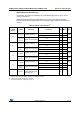
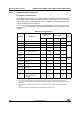
Output voltage levels
Unless otherwise specified, the parameters given in Table 44 are derived from tests
performed under ambient temperature and V
DD
supply voltage conditions summarized in
Table 14. All I/Os are CMOS and TTL compliant.
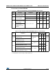
Table 44. Output voltage characteristics
Symbol Parameter Conditions Min Max Unit
V
OL
(1)(2)
Output low level voltage for an I/O pin
I
IO
= +8 mA
2.7 V < V
DD
< 3.6 V
-0.4
V
V
OH
(3)(2)
Output high level voltage for an I/O pin V
DD
-0.4 -
V
OL
(3)(4)
Output low level voltage for an I/O pin I
IO
=+ 4 mA
1.65 V < V
DD
<
2.7 V
-0.45
V
OH
(3)(4)
Output high level voltage for an I/O pin V
DD
-0.45 -
V
OL
(1)(4)
Output low level voltage for an I/O pin
I
IO
= +20 mA
2.7 V < V
DD
< 3.6 V
-1.3
V
OH
(3)(4)
Output high level voltage for an I/O pin V
DD
-1.3 -
1. The I
IO
current sunk by the device must always respect the absolute maximum rating specified in Table 12
and the sum of I
IO
(I/O ports and control pins) must not exceed I
VSS
.
2. Tested in production.
3. The I
IO
current sourced by the device must always respect the absolute maximum rating specified in
Table 12 and the sum of I
IO
(I/O ports and control pins) must not exceed I
VDD
.
4. Based on characterization data, not tested in production.