
Datasheet

DocID022799 Rev 6 85/132
STM32L15xCC STM32L15xRC STM32L15xUC STM32L15xVC Electrical characteristics
111
6.3.13 I/O port characteristics
General input/output characteristics
Unless otherwise specified, the parameters given in Table 43 are derived from tests
performed under the conditions summarized in Table 14. All I/Os are CMOS and TTL
compliant.
Output driving current
The GPIOs (general purpose input/outputs) can sink or source up to ±8 mA, and sink or
source up to ±20 mA with the non-standard V
OL
/V
OH
specifications given in Table 44.
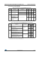
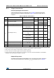
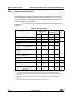
Table 43. I/O static characteristics
Symbol Parameter Conditions Min Typ
Max Unit
V
IL
Input low level voltage - - 0.3V
DD
(1)
VV
IH
Input high level voltage
Standard I/O
0.7 V
DD
--
FT I/O - -
V
hys
I/O Schmitt trigger voltage hysteresis
(2)
Standard I/O - 10% V
DD
(3)
-
I
lkg
Input leakage current
(4)
V
SS
V
IN
V
DD
I/Os with LCD
--±50
nA
V
SS
V
IN
V
DD
I/Os with analog switches
--±50
V
SS
V
IN
V
DD
I/Os with analog switches and
LCD
--±50
V
SS
V
IN
V
DD
I/Os with USB
--±250
V
SS
V
IN
V
DD
Standard I/Os
--±50
FT I/O
V
DD
≤ V
IN
≤ 5V
--±10uA
R
PU
Weak pull-up equivalent resistor
(5)(1)
V
IN
V
SS
30 45 60 k
R
PD
Weak pull-down equivalent resistor
(5)
V
IN
V
DD
30 45 60 k
C
IO
I/O pin capacitance - - - 5 - pF
1. Tested in production
2. Hysteresis voltage between Schmitt trigger switching levels. Based on characterization, not tested in production.
3. With a minimum of 200 mV. Based on characterization, not tested in production.
4. The max. value may be exceeded if negative current is injected on adjacent pins.
5. Pull-up and pull-down resistors are designed with a true resistance in series with a switchable PMOS/NMOS. This MOS/NMOS
contribution to the series resistance is minimum (~10% order).