
Datasheet

Electrical characteristics STM32L15xCC STM32L15xRC STM32L15xUC STM32L15xVC
80/132 DocID022799 Rev 6
6.3.8 PLL characteristics
The parameters given in Table 34 are derived from tests performed under ambient
temperature and V
DD
supply voltage conditions summarized in Table 14.
6.3.9 Memory characteristics
The characteristics are given at T
A
= -40 to 105 °C unless otherwise specified.
RAM memory
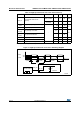
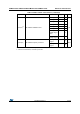
Table 34. PLL characteristics
Symbol Parameter
Value
Unit
Min Typ Max
(1)
1. Based on characterization, not tested in production.
f
PLL_IN
PLL input clock
(2)
2. Take care of using the appropriate multiplier factors so as to have PLL input clock values compatible with
the range defined by f
PLL_OUT
.
2- 24MHz
PLL input clock duty cycle 45 - 55 %
f
PLL_OUT
PLL output clock 2 - 32 MHz
t
LOCK
Worst case PLL lock time
PLL input = 2 MHz
PLL VCO = 96 MHz
- 100 130 µs
Jitter Cycle-to-cycle jitter -
600 ps
I
DDA
(PLL) Current consumption on V
DDA
- 220 450
µA
I
DD
(PLL) Current consumption on V
DD
- 120 150
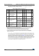
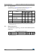
Table 35. RAM and hardware registers
Symbol Parameter Conditions Min Typ Max Unit
VRM Data retention mode
(1)
1. Minimum supply voltage without losing data stored in RAM (in Stop mode or under Reset) or in hardware
registers (only in Stop mode).
STOP mode (or RESET) 1.65 - - V