
Datasheet

DocID022799 Rev 6 57/132
STM32L15xCC STM32L15xRC STM32L15xUC STM32L15xVC Electrical characteristics
111
6.3.2 Embedded reset and power control block characteristics
The parameters given in the following table are derived from the tests performed under the
ambient temperature condition summarized in Table 14.
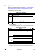
TA Temperature range
Maximum power
dissipation
–40 85
°C
Low power dissipation
(5)
–40 105
T
J Junction temperature range -40 °C T
A
105 °C –40 105 °C
1. When the ADC is used, refer to Table 56: ADC characteristics.
2. It is recommended to power V
DD
and V
DDA
from the same source. A maximum difference of 300 mV
between V
DD
and V
DDA
can be tolerated during power-up and up to 140 mV in operation.
3. To sustain a voltage higher than VDD+0.3V, the internal pull-up/pull-down resistors must be disabled
4. If T
A
is lower, higher P
D
values are allowed as long as T
J
does not exceed T
J
max (see Table 72: Thermal
characteristics on page 125).
5. In low power dissipation state, T
A
can be extended to this range as long as T
J
does not exceed T
J
max (see
Table 72: Thermal characteristics on page 125).
Table 14. General operating conditions (continued)
Symbol Parameter Conditions Min Max Unit
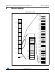
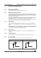
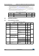
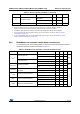
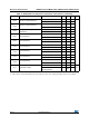
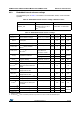
Table 15. Embedded reset and power control block characteristics
Symbol Parameter Conditions Min Typ
Max Unit
t
VDD
(1)
V
DD
rise time rate
BOR detector enabled 0 -
µs/V
BOR detector disabled 0 - 1000
V
DD
fall time rate
BOR detector enabled 20 -
BOR detector disabled 0 - 1000
T
RSTTEMPO
(1)
Reset temporization
V
DD
rising, BOR enabled - 2 3.3
ms
V
DD
rising, BOR disabled
(2)
0.4 0.7 1.6
V
POR/PDR
Power on/power down reset
threshold
Falling edge 1 1.5 1.65
V
Rising edge 1.3 1.5 1.65
V
BOR0
Brown-out reset threshold 0
Falling edge 1.67 1.7 1.74
Rising edge 1.69 1.76 1.8
V
BOR1
Brown-out reset threshold 1
Falling edge 1.87 1.93 1.97
Rising edge 1.96 2.03 2.07
V
BOR2
Brown-out reset threshold 2
Falling edge 2.22 2.30 2.35
Rising edge 2.31 2.41 2.44