
Datasheet

Electrical characteristics STM32L15xCC STM32L15xRC STM32L15xUC STM32L15xVC
56/132 DocID022799 Rev 6
6.3 Operating conditions
6.3.1 General operating conditions
4. Positive current injection is not possible on these I/Os. A negative injection is induced by V
IN
<V
SS
. I
INJ(PIN)
must never be exceeded. Refer to Table 11 for maximum allowed input voltage values.
5. A positive injection is induced by V
IN
> V
DD
while a negative injection is induced by V
IN
< V
SS
. I
INJ(PIN)
must never be exceeded. Refer to Table 11: Voltage characteristics for the maximum allowed input voltage
values.
6. When several inputs are submitted to a current injection, the maximum I
INJ(PIN)
is the absolute sum of the
positive and negative injected currents (instantaneous values).
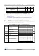
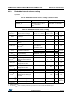
Table 13. Thermal characteristics
Symbol Ratings Value Unit
T
STG
Storage temperature range –65 to +150 °C
T
J
Maximum junction temperature 150 °C
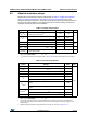
Table 14. General operating conditions
Symbol Parameter Conditions Min Max Unit
f
HCLK
Internal AHB clock frequency - 0 32
MHz
f
PCLK1
Internal APB1 clock
frequency
-0 32
f
PCLK2
Internal APB2 clock
frequency
-0 32
V
DD
Standard operating voltage
BOR detector disabled 1.65 3.6
V
BOR detector enabled,
at power on
1.8 3.6
BOR detector disabled,
after power on
1.65 3.6
V
DDA
(1)
Analog operating voltage
(ADC and DAC not used)
Must be the same voltage
as V
DD
(2)
1.65 3.6
V
Analog operating voltage
(ADC or DAC used)
1.8 3.6
V
IN
I/O input voltage
FT pins; 2.0 V V
DD
-0.3 5.5
(3)
V
FT pins; V
DD
2.0 V -0.3 5.25
(3)
BOOT0 pin 0 5.5
Any other pin -0.3 V
DD
+0.3
P
D
Power dissipation at
T
A
= 85 °C
(4)
UFBGA100 339 mW