
Datasheet

DocID022799 Rev 6 15/132
STM32L15xCC STM32L15xRC STM32L15xUC STM32L15xVC Functional overview
51
V
DD
=V
DDA
= 2.0 to 2.4 V
Conversion time
up to 500 Ksps
Functional
(2)
Range 1,
Range 2 or
Range 3
Full speed operation
V
DD
=V
DDA
= 2.4 to 3.6 V
Conversion time
up to 1 Msps
Functional
(2)
Range 1,
Range 2 or
Range 3
Full speed operation
1. CPU frequency changes from initial to final must respect "F
CPU
initial < 4*F
CPU
final" to limit V
CORE
drop due to
current consumption peak when frequency increases. It must also respect 5 µs delay between two changes. For
example to switch from 4.2 MHz to 32 MHz, you can switch from 4.2 MHz to 16 MHz, wait 5 µs, then switch from
16 MHz to 32 MHz.
2. Should be USB compliant from I/O voltage standpoint, the minimum V
DD
is 3.0 V.
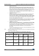
Table 3. Functionalities depending on the operating power supply range (continued)
Functionalities depending on the operating power supply range
Operating power supply
range
DAC and ADC
operation
USB
Dynamic voltage
scaling range
I/O operation
Table 4. CPU frequency range depending on dynamic voltage scaling
CPU frequency range Dynamic voltage scaling range
16 MHz to 32 MHz (1ws)
32 kHz to 16 MHz (0ws)
Range 1
8 MHz to 16 MHz (1ws)
32 kHz to 8 MHz (0ws)
Range 2
2.1MHz to 4.2 MHz (1ws)
32 kHz to 2.1 MHz (0ws)
Range 3