
Datasheet
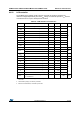


Package characteristics STM32L15xCC STM32L15xRC STM32L15xUC STM32L15xVC
120/132 DocID022799 Rev 6
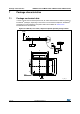
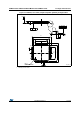
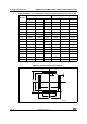
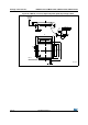
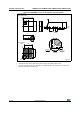
Figure 42. UFQFPN48 7 x 7 mm, 0.5 mm pitch, package outline
1. Drawing is not to scale.
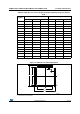
1. All leads/pads should also be soldered to the PCB to improve the lead/pad solder joint life.
1. There is an exposed die pad on the underside of the UFQFPN package. It is recommended to connect and
solder this back-side pad to PCB ground.
A0B9_ME_V3
D
Pin 1 identifier
laser marking area
EE
D
Y
D2
E2
Exposed pad
area
Z
1
48
Detail Z
R 0.125 typ.
1
48
L
C 0.500x45°
pin1 corner
A
Seating
plane
A1
b
e
ddd
Detail Y
T