
Datasheet

Electrical characteristics STM32L15xCC STM32L15xRC STM32L15xUC STM32L15xVC
110/132 DocID022799 Rev 6
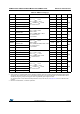
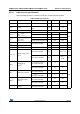
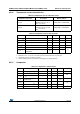
d
Voffset
/dt
Comparator offset
variation in worst voltage
stress conditions
V
DDA
3.6 V
V
IN+
0 V
V
IN-
V
REFINT
T
A
= 25 C
0 1.5 10 mV/1000 h
I
COMP1
Current consumption
(3)
- - 160 260 nA
1. Based on characterization, not tested in production.
2. The delay is characterized for 100 mV input step with 10 mV overdrive on the inverting input, the non-
inverting input set to the reference.
3. Comparator consumption only. Internal reference voltage not included.
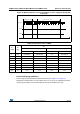
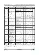
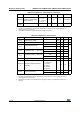
Table 64. Comparator 2 characteristics
Symbol Parameter Conditions Min Typ Max
(1)
1. Based on characterization, not tested in production.
Unit
V
DDA
Analog supply voltage - 1.65 - 3.6 V
V
IN
Comparator 2 input voltage range - 0 - V
DDA
V
t
START
Comparator startup time
Fast mode - 15 20
µs
Slow mode - 20 25
t
d slow
Propagation delay
(2)
in slow mode
2. The delay is characterized for 100 mV input step with 10 mV overdrive on the inverting input, the non-
inverting input set to the reference.
1.65 V V
DDA
2.7 V - 1.8 3.5
2.7 V V
DDA
3.6 V - 2.5 6
t
d fast
Propagation delay
(2)
in fast mode
1.65 V V
DDA
2.7 V - 0.8 2
2.7 V V
DDA
3.6 V - 1.2 4
V
offset
Comparator offset error - 4 20 mV
dThreshold/
dt
Threshold voltage temperature
coefficient
V
DDA
3.3V
T
A
= 0 to 50 C
V- =V
REFINT
,
3/4 V
REFINT
,
1/2 V
REFINT
,
1/4 V
REFINT
.
-15 30
ppm
/°C
I
COMP2
Current consumption
(3)
3. Comparator consumption only. Internal reference voltage (necessary for comparator operation) is not
included.
Fast mode - 3.5 5
µA
Slow mode - 0.5 2
Table 63. Comparator 1 characteristics (continued)
Symbol Parameter Conditions Min
(1)
Typ Max
(1)
Unit