
Datasheet
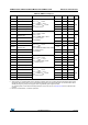

Electrical characteristics STM32L15xCC STM32L15xRC STM32L15xUC STM32L15xVC
108/132 DocID022799 Rev 6
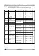
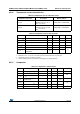
GBW Bandwidth
Normal mode
V
DD
>2.4 V
400 1000 3000
kHZ
Low power mode 150 300 800
Normal mode
V
DD
<2.4 V
200 500 2200
Low power mode 70 150 800
SR Slew rate
Normal mode
V
DD
>2.4 V
(between 0.1 V and
V
DD
-0.1 V)
- 700 -
V/ms
Low power mode V
DD
>2.4 V - 100 -
Normal mode
V
DD
<2.4 V
- 300 -
Low power mode - 50 -
AO Open loop gain
Normal mode 55 100 -
dB
Low power mode 65 110 -
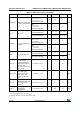
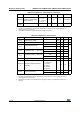
R
LOAD
Resistive load
Normal mode
V
DD
<2.4 V
4- -
k
Low power mode 20 - -
C
LOAD
Capacitive load - - - 50 pF
VOH
SAT
High saturation
voltage
Normal mode
I
LOAD
= max or
R
LOAD
= min
V
DD
-
100
--
mV
Low power mode V
DD
-50 - -
VOL
SAT
Low saturation
voltage
Normal mode - - 100
low power mode - - 50
m Phase margin - - 60 - °
GM Gain margin - - -12 - dB
t
OFFTRIM
Offset trim time: during calibration,
minimum time needed between two
steps to have 1 mV accuracy
--1-ms
t
WAKEUP
Wakeup time
Normal mode
C
LOAD
50 pf,
R
LOAD
4 k
-10-
µs
Low power mode
C
LOAD
50 pf,
R
LOAD
20 k
-30-
1. Operating conditions are limited to junction temperature (0 °C to 105 °C) when V
DD
is below 2 V. Otherwise, the operating
temperature range is 105 °C to -40 °C.
2. Data based on characterization results, not tested in production.
Table 60. Operational amplifier characteristics (continued)
Symbol Parameter Condition
(1)
Min
(2)
Typ Max
(2)
Unit