
Datasheet

DocID022799 Rev 6 107/132
STM32L15xCC STM32L15xRC STM32L15xUC STM32L15xVC Electrical characteristics
111
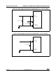
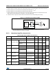
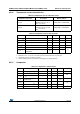
Figure 33. 12-bit buffered /non-buffered DAC
1. The DAC integrates an output buffer that can be used to reduce the output impedance and to drive external
loads directly without the use of an external operational amplifier. The buffer can be bypassed by
configuring the BOFFx bit in the DAC_CR register.
6.3.19 Operational amplifier characteristics
4. Difference between measured value at Code i and the value at Code i on a line drawn between Code 0 and last Code 4095.
5. Difference between the value measured at Code (0x800) and the ideal value = V
REF+
/2.
6. Difference between the value measured at Code (0x001) and the ideal value.
7. Difference between ideal slope of the transfer function and measured slope computed from code 0x000 and 0xFFF when
buffer is OFF, and from code giving 0.2 V and (V
DDA
– 0.2) V when buffer is ON.
8. In buffered mode, the output can overshoot above the final value for low input code (starting from min value).
R
LOAD
C
LOAD
Buffered/Non-buffered DAC
DAC_OUTx
Buffer(1)
12-bit
digital to
analog
converter
ai17157V2
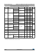
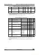
Table 60. Operational amplifier characteristics
Symbol Parameter Condition
(1)
Min
(2)
Typ Max
(2)
Unit
CMIR Common mode input range - 0 - V
DD
VI
OFFSET
Input offset voltage
Maximum
calibration range
---15
mV
After offset
calibration
---1.5
VI
OFFSET
Input offset voltage
drift
Normal mode - - - 40 µV/°C
Low power mode - - - 80
I
IB
Input current bias
Dedicated input
75 °C
--1
nA
General purpose
input
--10
I
LOAD
Drive current
Normal mode - - - 500
µA
Low power mode - - - 100
I
DD
Consumption
Normal mode
No load,
quiescent mode
- 100 220
µA
Low power mode - 30 60
CMRR
Common mode
rejection ration
Normal mode - - -85 -
dB
Low power mode - - -90 -
PSRR
Power supply
rejection ratio
Normal mode
DC
--85-
dB
Low power mode - -90 -