
Datasheet

Electrical characteristics STM32L15xCC STM32L15xRC STM32L15xUC STM32L15xVC
106/132 DocID022799 Rev 6
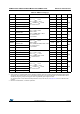
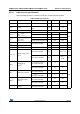
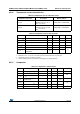
dOffset/dT
(1)
Offset error temperature
coefficient (code 0x800)
V
DDA
3.3V
V
REF+
3.0V
T
A
= 0 to 50 C
DAC output buffer OFF
-20 -10 0
µV/°C
V
DDA
3.3V
V
REF+
3.0V
T
A
= 0 to 50 C
DAC output buffer ON
020 50
Gain
(1)
Gain error
(7)
C
L
50 pF, R
L
5 k
DAC output buffer ON
- +0.1 / -0.2% +0.2 / -0.5%
%
No R
LOAD
, C
L
50 pF
DAC output buffer OFF
- +0 / -0.2% +0 / -0.4%
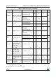
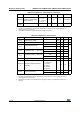
dGain/dT
(1)
Gain error temperature
coefficient
V
DDA
3.3V
V
REF+
3.0V
T
A
= 0 to 50 C
DAC output buffer OFF
-10 -2 0
µV/°C
V
DDA
3.3V
V
REF+
3.0V
T
A
= 0 to 50 C
DAC output buffer ON
-40 -8 0
TUE
(1)
Total unadjusted error
C
L
50 pF, R
L
5 k
DAC output buffer ON
-12 30
LSB
No R
LOAD
, C
L
50 pF
DAC output buffer OFF
-8 12
t
SETTLING
Settling time (full scale:
for a 12-bit code
transition between the
lowest and the highest
input codes till
DAC_OUT reaches final
value ±1LSB
C
L
50 pF, R
L
5 k - 7 12 µs
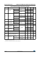
Update rate
Max frequency for a
correct DAC_OUT
change (95% of final
value) with 1 LSB
variation in the input
code
C
L
50 pF, R
L
5 k - - 1 Msps
t
WAKEUP
Wakeup time from off
state (setting the ENx bit
in the DAC Control
register)
(8)
C
L
50 pF, R
L
5 k - 9 15 µs
PSRR+
V
DDA
supply rejection
ratio (static DC
measurement)
C
L
50 pF, R
L
5 k - -60 -35 dB
1. Data based on characterization results.
2. Connected between DAC_OUT and V
SSA
.
3. Difference between two consecutive codes - 1 LSB.
Table 59. DAC characteristics (continued)
Symbol Parameter Conditions Min Typ Max Unit