
Datasheet
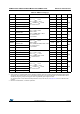
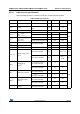
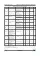
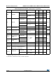

Electrical characteristics STM32L15xCC STM32L15xRC STM32L15xUC STM32L15xVC
102/132 DocID022799 Rev 6
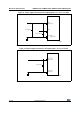
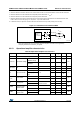
Figure 28. ADC accuracy characteristics
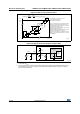
Figure 29. Typical connection diagram using the ADC
1. Refer to Table 58: RAIN max for fADC = 16 MHz for the value of R
AIN
and Table 56: ADC characteristics
for the value of C
ADC
.
2. C
parasitic
represents the capacitance of the PCB (dependent on soldering and PCB layout quality) plus the
pad capacitance (roughly 7
pF). A high C
parasitic
value will downgrade conversion accuracy. To remedy
this, f
ADC
should be reduced.
E
O
E
G
1LSB
IDEAL
(1) Example of an actual transfer curve
(2) The ideal transfer curve
(3) End point correlation line
E
T
=Total Unadjusted Error: maximum devia tion
between the actual and the ideal transfer curves.
E
O
=Offset Error: deviation between the first actual
transition and the first ideal one.
E
G
=Gain Error: deviation between the last ideal
transition and the last actual one.
E
D
=Differential Linearity Error: maximum deviation
between actual steps and the ideal one.
E
L
=Integral Linearity Error: maximum deviation
between any actual transition and the end point
correlation line.
4095
4094
4093
5
4
3
2
1
0
7
6
1234567
4093 4094 4095 4096
(1)
(2)
E
T
E
D
E
L
(3)
V
DDA
V
SSA
ai14395b
V
REF+
4096
(or depending on package)]
V
DDA
4096
[1LSB
IDEAL
=
ai17856c
STM32L15xxx
VDD
AINx
IL± 50 nA
0.6 V
VT
R
AIN
(1)
C
parasitic
VAIN
0.6 V
VT
12-bit
converter
C
ADC
(1)
Sample and hold ADC
converter