
Datasheet


Electrical characteristics STM32L151x6/8/B, STM32L152x6/8/B
96/131 DocID17659 Rev 9
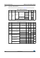
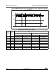
Table 55. ADC accuracy
(1)(2)
Symbol Parameter Test conditions Min
(3)
Typ Max
(3)
Unit
ET Total unadjusted error
2.4 V ≤ V
DDA
≤ 3.6 V
2.4 V ≤ V
REF+
≤ 3.6 V
f
ADC
= 8 MHz, R
AIN
= 50 Ω
T
A
= -40 to 105 °C
-24
LSB
EO Offset error - 1 2
EG Gain error - 1.5 3.5
ED Differential linearity error - 1 2
EL Integral linearity error - 1.7 3
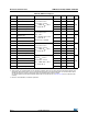
ENOB Effective number of bits
2.4 V ≤ V
DDA
≤ 3.6 V
V
DDA =
V
REF+
f
ADC
= 16 MHz, R
AIN
= 50 Ω
T
A
= -40 to 105 °C
1 kHz ≤ F
input
≤ 100 kHz
9.2 10 - bits
SINAD
Signal-to-noise and
distortion ratio
57.5 62 -
dB
SNR Signal-to-noise ratio 57.5 62 -
THD Total harmonic distortion -74 -75 -
ET Total unadjusted error
2.4 V ≤ V
DDA
≤ 3.6 V
1.8 V ≤
V
REF+
≤ 2.4 V
f
ADC
= 4 MHz, R
AIN
= 50 Ω
T
A
= -40 to 105 °C
-46.5
LSB
EO Offset error - 2 4
EG Gain error - 4 6
ED Differential linearity error - 1 2
EL Integral linearity error - 1.5 3
ET Total unadjusted error
1.8 V ≤
V
DDA
≤ 2.4 V
1.8 V ≤ V
REF+
≤ 2.4 V
f
ADC
= 4 MHz, R
AIN
= 50 Ω
T
A
= -40 to 105 °C
-23
LSB
EO Offset error - 1 1.5
EG Gain error - 1.5 2
ED Differential linearity error - 1 2
EL Integral linearity error - 1 1.5
1. ADC DC accuracy values are measured after internal calibration.
2. ADC accuracy vs. negative injection current: Injecting a negative current on any analog input pins should be avoided as this
significantly reduces the accuracy of the conversion being performed on another analog input. It is recommended to add a
Schottky diode (pin to ground) to analog pins which may potentially inject negative currents.
Any positive injection current within the limits specified for I
INJ(PIN)
and ΣI
INJ(PIN)
in Section 6.3.12 does not affect the ADC
accuracy.
3. Based on characterization, not tested in production.