
Datasheet


Electrical characteristics STM32L151x6/8/B, STM32L152x6/8/B
86/131 DocID17659 Rev 9
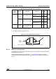
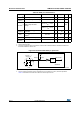
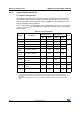
Figure 20. Recommended NRST pin protection
1. The reset network protects the device against parasitic resets.
2. The user must ensure that the level on the NRST pin can go below the V
IL(NRST)
max level specified in
Table 45. Otherwise the reset will not be taken into account by the device.
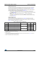
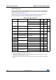
Table 45. NRST pin characteristics
Symbol Parameter Conditions Min Typ Max Unit
V
IL(NRST)
(1)
1. Guaranteed by design, not tested in production.
NRST input low level voltage - - - 0.8
V
V
IH(NRST)
(1)
NRST input high level voltage - 1.4 -
V
OL(NRST)
(1)
NRST output low level
voltage
I
OL
= 2 mA
2.7 V < V
DD
< 3.6 V
--
0.4
I
OL
= 1.5 mA
1.65 V < V
DD
< 2.7 V
--
V
hys(NRST)
(1)
NRST Schmitt trigger voltage
hysteresis
--10%V
DD
(2)
2. 200 mV minimum value
mV
R
PU
Weak pull-up equivalent
resistor
(3)
3. The pull-up is designed with a true resistance in series with a switchable PMOS. This PMOS contribution to
the series resistance is around 10%.
V
IN
= V
SS
30 45 60 kΩ
V
F(NRST)
(1)
NRST input filtered pulse - - - 50 ns
V
NF(NRST)
(1)
NRST input not filtered pulse - 350 - ns
ai17854
STM32Lxx
R
PU
NRST
(2)
V
DD
Filter
Internal reset
0.1 μF
External
reset circuit
(1)