
Datasheet


Pin descriptions STM32L151x6/8/B, STM32L152x6/8/B
40/131 DocID17659 Rev 9
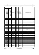
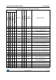
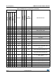
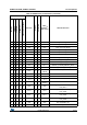
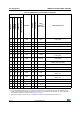
83 54 B5 C8 - PD2 I/O FT PD2
TIM3_ETR/LCD_SEG31/LCD_SEG43/
LCD_COM7
84 - - B8 - PD3 I/O FT PD3 USART2_CTS/SPI2_MISO
85 - - B7 - PD4 I/O FT PD4 USART2_RTS/SPI2_MOSI
86 - - A6 - PD5 I/O FT PD5 USART2_TX
87 - - B6 - PD6 I/O FT PD6 USART2_RX
88 - - A5 - PD7 I/O FT PD7 USART2_CK/TIM9_CH2
89 55 A5 A8 39 PB3 I/O FT JTDO
TIM2_CH2/PB3/SPI1_SCK/COMP2_INM/
LCD_SEG7
90 56 A4 A7 40 PB4 I/O FT NJTRST
TIM3_CH1/PB4/SPI1_MISO/COMP2_INP/
LCD_SEG8
91 57 C4 C5 41 PB5 I/O FT PB5
I2C1_SMBA/TIM3_CH2/SPI1_MOSI/
COMP2_INP/LCD_SEG9
92 58 D3 B5 42 PB6 I/O FT PB6 I2C1_SCL/TIM4_CH1/USART1_TX
93 59 C3 B4 43 PB7 I/O FT PB7 I2C1_SDA/TIM4_CH2/USART1_RX/PVD_IN
94 60 B4 A4 44 BOOT0 I B BOOT0 -
95 61 B3 A3 45 PB8 I/O FT PB8
TIM4_CH3/I2C1_SCL/LCD_SEG16/
TIM10_CH1
96 62 A3 B3 46 PB9 I/O FT PB9
TIM4_CH4/I2C1_SDA/LCD_COM3/
TIM11_CH1
97 - - C3 - PE0 I/O FT PE0 TIM4_ETR/LCD_SEG36/TIM10_CH1
98 - - A2 - PE1 I/O FT PE1 LCD_SEG37/TIM11_CH1
99 63 D4 D3 47 V
SS_3
S- V
SS_3
-
100 64 E4 C4 48 V
DD_3
S- V
DD_3
-
1. I = input, O = output, S = supply.
2. Function availability depends on the chosen device. For devices having reduced peripheral counts, it is always the lower
number of peripheral that is included. For example, if a device has only one SPI and two USARTs, they will be called SPI1
and USART1 & USART2, respectively. Refer to Table 2 on page 10.
3. Applicable to STM32L152xx devices only. In STM32L151xx devices, this pin should be connected to V
DD
.
Table 8. STM32L15xxx pin definitions (continued)
Pins
Pin name
Pin type
(1)
I/O structure
Main
function
(2)
(after reset)
Alternate functions
LQFP100
LQFP64
TFBGA64
UFBGA100
LQFP48 or UFQFPN48