
Datasheet


DocID17659 Rev 9 93/131
STM32L151x6/8/B, STM32L152x6/8/B Electrical characteristics
105
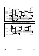
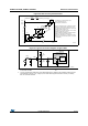
Figure 25. USB timings: definition of data signal rise and fall time
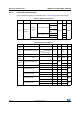
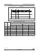
Table 51. USB DC electrical characteristics
Symbol Parameter Conditions Min.
(1)
1. All the voltages are measured from the local ground potential.
Max.
(1)
Unit
Input levels
V
DD
USB operating voltage
(2)
2. To be compliant with the USB 2.0 full speed electrical specification, the USB_DP (D+) pin should be pulled
up with a 1.5 kΩ resistor to a 3.0-to-3.6 V voltage range.
-3.03.6V
V
DI
(3)
3. Guaranteed by characterization, not tested in production.
Differential input sensitivity I(USB_DP, USB_DM) 0.2 -
VV
CM
(3)
Differential common mode range Includes V
DI
range 0.8 2.5
V
SE
(3)
Single ended receiver threshold - 1.3 2.0
Output levels
V
OL
(4)
4. Tested in production.
Static output level low R
L
of 1.5 kΩ to 3.6 V
(5)
5.
R
L
is the load connected on the USB drivers.
-0.3
V
V
OH
(4)
Static output level high R
L
of 15 kΩ to V
SS
(5)
2.8 3.6
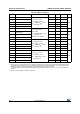
Table 52. USB: full speed electrical characteristics
Driver characteristics
(1)
1. Guaranteed by design, not tested in production.
Symbol Parameter Conditions Min Max Unit
t
r
Rise time
(2)
2.
Measured from 10% to 90% of the data signal. For more detailed informations, please refer to USB
Specification - Chapter 7 (version 2.0).
C
L
= 50 pF
420ns
t
f
Fall Time
(2)
C
L
= 50 pF 4 20 ns
t
rfm
Rise/ fall time matching t
r
/t
f
90 110 %
V
CRS
Output signal crossover voltage 1.3 2.0 V
ai14137
t
f
Differen tial
Data L ines
V
SS
V
CR S
t
r
Crossover
points