
Datasheet


Electrical characteristics STM32L151x6/8/B, STM32L152x6/8/B
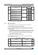
78/131 DocID17659 Rev 9
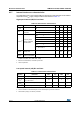
6.3.10 EMC characteristics
Susceptibility tests are performed on a sample basis during device characterization.
Functional EMS (electromagnetic susceptibility)
While a simple application is executed on the device (toggling 2 LEDs through I/O ports).
the device is stressed by two electromagnetic events until a failure occurs. The failure is
indicated by the LEDs:
• Electrostatic discharge (ESD) (positive and negative) is applied to all device pins until
a functional disturbance occurs. This test is compliant with the IEC 61000-4-2 standard.
• FTB: A Burst of Fast Transient voltage (positive and negative) is applied to V
DD
and
V
SS
through a 100 pF capacitor, until a functional disturbance occurs. This test is
compliant with the IEC 61000-4-4 standard.
A device reset allows normal operations to be resumed.
The test results are given in Table 37. They are based on the EMS levels and classes
defined in application note AN1709.
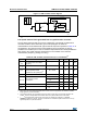
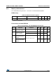
Table 36. Flash memory, data EEPROM endurance and data retention
Symbol Parameter Conditions
Value
Unit
Min
(1)
1. Based on characterization not tested in production.
Typ Max
NCYC
(2)
Cycling (erase / write)
Program memory
T
A
= -40°C to
105 °C
10
--
kcycles
Cycling (erase / write)
EEPROM data memory
300 - -
t
RET
(2)
2. Characterization is done according to JEDEC JESD22-A117.
Data retention (program memory) after
10 kcycles at T
A
= 85 °C
TRET = +85 °C
30 - -
years
Data retention (EEPROM data memory)
after 300 kcycles at T
A
= 85 °C
30 - -
Data retention (program memory) after
10 kcycles at T
A
= 105 °C
TRET = +105 °C
10 - -
Data retention (EEPROM data memory)
after 300 kcycles at T
A
= 105 °C
10 - -
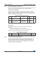
Table 37. EMS characteristics
Symbol Parameter Conditions
Level/
Class
V
FESD
Voltage limits to be applied on any I/O pin to
induce a functional disturbance
V
DD
= 3.3 V, LQFP100, T
A
= +25 °C,
f
HCLK
= 32 MHz
conforms to IEC 61000-4-2
2B
V
EFTB
Fast transient voltage burst limits to be
applied through 100 pF on V
DD
and V
SS
pins to induce a functional disturbance
V
DD
= 3.3 V, LQFP100, T
A
= +25 °C,
f
HCLK
= 32 MHz
conforms to IEC 61000-4-4
4A