
Datasheet


Electrical characteristics STM32L151x6/8/B, STM32L152x6/8/B
68/131 DocID17659 Rev 9
All timings are derived from tests performed under ambient temperature and V
DD
supply
voltage conditions summarized in Table 13.
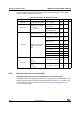
6.3.6 External clock source characteristics
High-speed external user clock generated from an external source
In bypass mode the HSE oscillator is switched off and the input pin is a standard GPIO. The
external clock signal has to respect the I/O characteristics in Section 6.3.13. However, the
recommended clock input waveform is shown in Figure 15: High-speed external clock
source AC timing diagram.
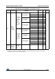
Table 25. Low-power mode wakeup timings
Symbol Parameter Conditions Typ Max
(1)
1. Based on characterization, not tested in production, unless otherwise specified
Unit
t
WUSLEEP
Wakeup from Sleep mode f
HCLK
= 32 MHz 0.36 -
µs
t
WUSLEEP_LP
Wakeup from Low power
sleep mode
f
HCLK
= 262 kHz
f
HCLK
= 262 kHz
Flash enabled
32 -
f
HCLK
= 262 kHz
Flash switched OFF
34 -
t
WUSTOP
Wakeup from Stop mode,
regulator in Run mode
f
HCLK
= f
MSI
= 4.2 MHz 8.2 -
Wakeup from Stop mode,
regulator in low power
mode
f
HCLK
= f
MSI
= 4.2 MHz
Voltage Range 1 and 2
8.2 9.3
f
HCLK
= f
MSI
= 4.2 MHz
Voltage Range 3
7.8 11.2
f
HCLK
= f
MSI
= 2.1 MHz 10 12
f
HCLK
= f
MSI
= 1.05 MHz 15.5 20
f
HCLK
= f
MSI
= 524 kHz 29 35
f
HCLK
= f
MSI
= 262 kHz 53 63
f
HCLK
= f
MSI
= 131 kHz 105 118
f
HCLK
= MSI = 65 kHz 210 237
t
WUSTDBY
Wakeup from Standby
mode
FWU bit = 1
f
HCLK
= MSI = 2.1 MHz 50 103
Wakeup from Standby
mode
FWU bit = 0
f
HCLK
= MSI = 2.1 MHz 2.5 3.2 ms