
Datasheet


Electrical characteristics STM32L151x6/8/B, STM32L152x6/8/B
52/131 DocID17659 Rev 9
6.3 Operating conditions
6.3.1 General operating conditions
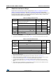
Table 12. Thermal characteristics
Symbol Ratings Value Unit
T
STG
Storage temperature range –65 to +150 °C
T
J
Maximum junction temperature 150 °C
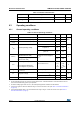
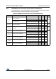
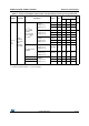
Table 13. General operating conditions
Symbol Parameter Conditions Min Max Unit
f
HCLK
Internal AHB clock frequency - 0 32
MHzf
PCLK1
Internal APB1 clock frequency - 0 32
f
PCLK2
Internal APB2 clock frequency - 0 32
V
DD
Standard operating voltage
BOR detector disabled 1.65 3.6
V
BOR detector enabled,
at power on
1.8 3.6
BOR detector disabled, after
power on
1.65 3.6
V
DDA
(1)
Analog operating voltage
(ADC and DAC not used)
Must be the same voltage as
V
DD
(2)
1.65 3.6
V
Analog operating voltage
(ADC or DAC used)
1.8 3.6
V
IN
Input voltage on FT pins
(3)
Input voltage on BOOT0 pin
Input voltage on any other pin
2.0 V ≤V
DD
≤ 3.6 V
1.65 V ≤ V
DD
≤ 2.0 V
–0.3
–0.3
0
–0.3
5.5
5.25
5.5
V
DD
+0.3
V
P
D
Power dissipation at
T
A
= 85 °C
(4)
BGA100 package - 339 mW
TA Temperature range
Maximum power dissipation –40 85
°C
Low power dissipation
(5)
–40 105
T
J Junction temperature range -40 °C ≤ T
A
≤ 105°C –40 105 °C
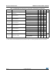
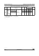
1. When the ADC is used, refer to Table 54: ADC characteristics.
2. It is recommended to power V
DD
and V
DDA
from the same source. A maximum difference of 300 mV between V
DD
and
V
DDA
can be tolerated during power-up and operation.
3. To sustain a voltage higher than V
DD
+0.3 V, the internal pull-up/pull-down resistors must be disabled.
4. If T
A
is lower, higher P
D
values are allowed as long as T
J
does not exceed T
J
max (see Table 12: Thermal characteristics
on page 52).
5. In low power dissipation state, T
A
can be extended to this range as long as T
J
does not exceed T
J
max (see Table 12:
Thermal characteristics on page 52).