
Datasheet


DocID17659 Rev 9 51/131
STM32L151x6/8/B, STM32L152x6/8/B Electrical characteristics
105
6.2 Absolute maximum ratings
Stresses above the absolute maximum ratings listed in Table 10: Voltage characteristics,
Table 11: Current characteristics, and Table 12: Thermal characteristics may cause
permanent damage to the device. These are stress ratings only and functional operation of
the device at these conditions is not implied. Exposure to maximum rating conditions for
extended periods may affect device reliability.
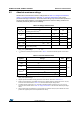
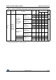
Table 10. Voltage characteristics
Symbol Ratings Min Max Unit
V
DD
–V
SS
External main supply voltage
(including V
DDA
and V
DD
)
(1)
1. All main power (V
DD
, V
DDA
) and ground (V
SS
, V
SSA
) pins must always be connected to the external power
supply, in the permitted range.
–0.3 4.0
V
V
IN
(2)
2. V
IN
maximum must always be respected. Refer to Table 11 for maximum allowed injected current values.
Input voltage on five-volt tolerant pin V
SS
− 0.3 V
DD
+4.0
Input voltage on any other pin V
SS
− 0.3 4.0
|ΔV
DDx
| Variations between different V
DD
power pins - 50
mV
|V
SSX
− V
SS
| Variations between all different ground pins - 50
V
REF+
− V
DDA
Allowed voltage difference for V
REF+
> V
DDA
-0.4V
V
ESD(HBM)
Electrostatic discharge voltage
(human body model)
see Section 6.3.11 -
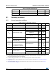
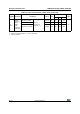
Table 11. Current characteristics
Symbol Ratings Max. Unit
I
VDDΣ
Total current into V
DD
/V
DDA
power lines (source)
(1)
1. All main power (V
DD
, V
DDA
) and ground (V
SS
, V
SSA
) pins must always be connected to the external power
supply, in the permitted range.
80
mA
I
VSSΣ
Total current out of V
SS
ground lines (sink)
(1)
80
I
IO
Output current sunk by any I/O and control pin 25
Output current sourced by any I/O and control pin - 25
I
INJ(PIN)
(2)
2. Negative injection disturbs the analog performance of the device. See note in Section 6.3.17.
Injected current on five-volt tolerant I/O
(3)
3. Positive current injection is not possible on these I/Os. A negative injection is induced by V
IN
<V
SS
. I
INJ(PIN)
must never be exceeded. Refer to Table 10 for maximum allowed input voltage values.
-5/+0
Injected current on any other pin
(4)
4. A positive injection is induced by V
IN
> V
DD
while a negative injection is induced by V
IN
< V
SS
. I
INJ(PIN)
must never be exceeded. Refer to Table 10: Voltage characteristics for the maximum allowed input voltage
values.
± 5
ΣI
INJ(PIN)
Total injected current (sum of all I/O and control pins)
(5)
5. When several inputs are submitted to a current injection, the maximum ΣI
INJ(PIN)
is the absolute sum of the
positive and negative injected currents (instantaneous values).
± 25