
Datasheet

Functional overview STM32L151x6/8/B, STM32L152x6/8/B
14/131 DocID17659 Rev 9
HSE crystal oscillators are disabled. The voltage regulator is in the low power mode.
The device can be woken up from Stop mode by any of the EXTI line, in 8 µs. The EXTI
line source can be one of the 16 external lines. It can be the PVD output, the
Comparator 1 event or Comparator 2 event (if internal reference voltage is on). It can
also be wakened by the USB wakeup.
Stop mode consumption: refer to Table 22: Typical and maximum current
consumptions in Stop mode.
• Standby mode with RTC
Standby mode is used to achieve the lowest power consumption and real time clock.
The internal voltage regulator is switched off so that the entire V
CORE
domain is
powered off. The PLL, MSI RC, HSI RC and HSE crystal oscillators are also switched
off. The LSE or LSI is still running. After entering Standby mode, the RAM and register
contents are lost except for registers in the Standby circuitry (wakeup logic, IWDG,
RTC, LSI, LSE Crystal 32K osc, RCC_CSR).
The device exits Standby mode in 60 µs when an external reset (NRST pin), an IWDG
reset, a rising edge on one of the three WKUP pins, RTC alarm (Alarm A or Alarm B),
RTC tamper event, RTC timestamp event or RTC Wakeup event occurs.
• Standby mode without RTC
Standby mode is used to achieve the lowest power consumption. The internal voltage
regulator is switched off so that the entire V
CORE
domain is powered off. The PLL, MSI,
RC, HSI and LSI RC, HSE and LSE crystal oscillators are also switched off. After
entering Standby mode, the RAM and register contents are lost except for registers in
the Standby circuitry (wakeup logic, IWDG, RTC, LSI, LSE Crystal 32K osc,
RCC_CSR).
The device exits Standby mode in 60 µs when an external reset (NRST pin) or a rising
edge on one of the three WKUP pin occurs.
Standby mode consumption: refer to Table 23.
Note: The RTC, the IWDG, and the corresponding clock sources are not stopped by entering the
Stop or Standby mode.
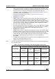
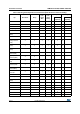
Table 3. Functionalities depending on the operating power supply range
Operating power
supply range
Functionalities depending on the operating power supply range
DAC and ADC
operation
USB
Dynamic voltage
scaling range
I/O operation
V
DD
= 1.65 to 1.71 V Not functional Not functional
Range 2 or
Range 3
Degraded speed
performance
V
DD
= 1.71 to 1.8 V
(1)
Not functional Not functional
Range 1,
Range 2 or
Range 3
Degraded speed
performance
V
DD
= 1.8 to 2.0 V
(1)
Conversion time
up to 500 Ksps
Not functional
Range 1,
Range 2 or
Range 3
Degraded speed
performance