
Datasheet


DocID022152 Rev 4 131/185
STM32F405xx, STM32F407xx Electrical characteristics
a
Note: ADC accuracy vs. negative injection current: injecting a negative current on any analog
input pins should be avoided as this significantly reduces the accuracy of the conversion
being performed on another analog input. It is recommended to add a Schottky diode (pin to
ground) to analog pins which may potentially inject negative currents.
Any positive injection current within the limits specified for I
INJ(PIN)
and ΣI
INJ(PIN)
in
Section 5.3.16 does not affect the ADC accuracy.
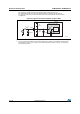
Figure 50. ADC accuracy characteristics
1. See also Table 68.
2. Example of an actual transfer curve.
3. Ideal transfer curve.
4. End point correlation line.
5. E
T
= Total Unadjusted Error: maximum deviation between the actual and the ideal transfer curves.
EO = Offset Error: deviation between the first actual transition and the first ideal one.
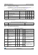
Table 68. ADC accuracy at f
ADC
= 30 MHz
(1)
1. Better performance could be achieved in restricted V
DD
, frequency and temperature ranges.
Symbol Parameter Test conditions Typ Max
(2)
2. Based on characterization, not tested in production.
Unit
ET Total unadjusted error
f
PCLK2
= 60 MHz,
f
ADC
= 30 MHz, R
AIN
< 10 kΩ,
V
DDA
= 1.8
(3)
to 3.6 V
3. V
DD
/V
DDA
minimum value of 1.7 V is obtained when the device operates in reduced temperature range,
and with the use of an external power supply supervisor (refer to Section : Internal reset OFF).
±2 ±5
LSB
EO Offset error ±1.5 ±2.5
EG Gain error ±1.5 ±3
ED Differential linearity error ±1 ±2
EL Integral linearity error ±1.5 ±3
ai14395c
E
O
E
G
1L SB
IDEAL
4095
4094
4093
5
4
3
2
1
0
7
6
1 2 3 456 7
4093 4094 4095 4096
(1)
(2)
E
T
E
D
E
L
(3)
V
DDA
V
SSA
V
REF+
4096
(or depending on package)]
V
DDA
4096
[1LSB
IDEAL
=