
Datasheet

Electrical characteristics STM32F37xxx
84/131 DocID022691 Rev 4
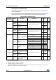
6.3.14 I/O port characteristics
General input/output characteristics
Unless otherwise specified, the parameters given in Table 52 are derived from tests
performed under the conditions summarized in Table 22. All I/Os are CMOS and TTL
compliant.
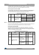
Table 52. I/O static characteristics
(1)
Symbol Parameter Conditions Min Typ Max Unit
V
IL
Low level input
voltage
TC and TTa I/O - - 0.3V
DD
+0.07
(2)
V
FT and FTf I/O - - 0.475V
DD
–0.2
(2)
BOOT0 - - 0.3V
DD
–0.3
(2)
All I/Os except BOOT0 pin - - 0.3V
DD
V
IH
High level input
voltage
TC and TTa I/O 0.445V
DD
+0.398
(2)
--
FT and FTf I/O 0.5V
DD+0.2
(2)
--
BOOT0 0.2V
DD
+0.95
(2)
--
All I/Os except BOOT0 pin 0.7V
DD
--
V
hys
Schmitt trigger
hysteresis
TC and TTa I/O - 200
(2)
-
mVFT and FTf I/O - 100
(2)
-
BOOT0 - 300
(2)
-
I
lkg
Input leakage
current
(3)
TC, FT and FTf I/O
TTa in digital mode
V
SS
< V
IN
< V
DD
--±0.1
µA
TTa in digital mode
V
DD
≤ V
IN
≤ V
DDA
--1
TTa in analog mode
V
SS
≤ V
IN
≤ V
DDA
--±0.2
FT and FTf I/O
(3)
V
DD
≤ V
IN
≤ 5 V
--10
R
PU
Weak pull-up
equivalent
resistor
(4)
V
IN
= V
SS
25 40 55
kΩ
R
PD
Weak pull-down
equivalent
resistor
(4)
V
IN
= V
DD
25 40 55
C
IO
I/O pin capacitance - 5 - pF
1. VDDSD12 is the external power supply for the PB2, PB10, and PE7 to PE15 I/O pins (the I/O pin ground is internally
connected to VSS). VDDSD3 is the external power supply for PB14 to PB15 and PD8 to PD15 I/O pins (the I/O pin ground
is internally connected to VSS). For those pins all V
DD
supply references in this table are related to their given VDDSDx
power supply.
2. Data based on design simulation only. Not tested in production.
3. Leakage could be higher than maximum value, if negative current is injected on adjacent pins.
4. Pull-up and pull-down resistors are designed with a true resistance in series with a switchable PMOS/NMOS. This
PMOS/NMOS contribution to the series resistance is minimal (~10% order).