
Datasheet

DocID022691 Rev 4 81/131
STM32F37xxx Electrical characteristics
114
To complete these trials, ESD stress can be applied directly on the device, over the range of
specification values. When unexpected behavior is detected, the software can be hardened
to prevent unrecoverable errors occurring (see application note AN1015).
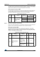
Electromagnetic Interference (EMI)
The electromagnetic field emitted by the device are monitored while a simple application is
executed (toggling 2 LEDs through the I/O ports). This emission test is compliant with
IEC 61967-2 standard which specifies the test board and the pin loading.
6.3.12 Electrical sensitivity characteristics
Based on three different tests (ESD, LU) using specific measurement methods, the device is
stressed in order to determine its performance in terms of electrical sensitivity.
Electrostatic discharge (ESD)
Electrostatic discharges (a positive then a negative pulse separated by 1 second) are
applied to the pins of each sample according to each pin combination. The sample size
depends on the number of supply pins in the device (3 parts × (n+1) supply pins). This test
conforms to the JESD22-A114/C101 standard.
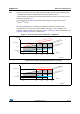
Table 48. EMI characteristics
Symbol Parameter Conditions
Monitored
frequency band
Max vs. [f
HSE
/f
HCLK
]
Unit
8/72 MHz
S
EMI
Peak level
V
DD
= 3.3 V, T
A
= 25 °C,
LQFP100 package
compliant with IEC
61967-2
0.1 to 30 MHz 9
dBµV30 to 130 MHz 26
130 MHz to 1 GHz 30
SAE EMI Level 4 -
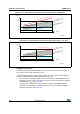
Table 49. ESD absolute maximum ratings
Symbol Ratings Conditions Class
Maximum
value
(1)
1. Data based on characterization results, not tested in production.
Unit
V
ESD(HBM
)
Electrostatic discharge
voltage (human body model)
T
A
= +25 °C,
conforming to JESD22-
A114
22000
V
V
ESD(CD
M)
Electrostatic discharge
voltage (charge device
model)
T
A
= +25 °C,
conforming to
ANSI/ESD STM5.3.1,
LQFP100, LQFP64,
LQFP48 and BGA100
packages
II 500
T
A
= +25 °C,
conforming to JESD22-
C101, WLCSP66
package
II 250