
Datasheet

DocID022691 Rev 4 53/131
STM32F37xxx Electrical characteristics
114
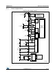
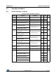
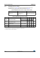
6.1.6 Power supply scheme
Figure 9. Power supply scheme
1. Dotted lines represent the internal connections on low pin count packages, joining the dedicated supply
pins.
MS19232V3
Analog:
RCs, PLL, COMP,
...
Power switch
V
BAT
GP I/O s
OUT
IN
Kernel logic
(CPU,
Digital
& Memories)
Backup circuitry
(LSE,RTC,
Backup registers)
Wakeup logic
2 × 100 nF
+ 1 × 4.7 μF
1.
65 - 3.6 V
Regulator
V
DDA
V
SSA
ADC/
DAC
Level shifter
IO
Logic
V
DD
10 nF
+ 1 μF
V
DDA
V
REF+
V
REF-
V
DD
V
SS
3 ×
2 ×
Sigma
Delta
ADCs
10 nF
+ 1 μF
VDDSD12
VDDSD12
VDDSD3
VDDSD3
VSSSD
10 nF
+ 1 μF
VREFSD+
VREFSD-
10 nF
+ 1 μF
VREFSD+
GP I/O s
OUT
IN
Level shifter
IO
Logic
GP I/O s
OUT
IN
Level shifter
IO
Logic
10 nF
+ 1 μF
V
REF
REF+
V
1.8 V
@V
DD
@VDDSD3
@VDDSD12