
Datasheet


Electrical characteristics STM32F37xxx
114/131 DocID022691 Rev 4
1. Data based on characterization results, not tested in production.
2. For f
ADC
lower than 5 MHz, there will be a performance degradation of around 2 dB due to flicker noise increase.
3. If the reference value is lower than 2.4 V, there will be a performance degradation proportional to the reference supply drop,
according to this formula: 20*log10(V
REF
/2.4) dB
4. SNR, THD, SINAD parameters are valid for frequency bandwidth 20Hz - 1kHz. Input signal frequency is 300Hz (for
f
ADC
=6MHz) and 100Hz (for f
ADC
=1.5MHz).
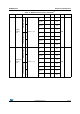
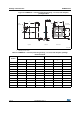
Table 75. VREFSD+ pin characteristics
(1)
Symbol Parameter Conditions Min Typ Max Unit Note
V
REFINT
Internal reference
voltage
Buffered embedded
reference voltage (1.2 V)
-1.2- V
See Section 6.3.4:
Embedded
reference voltage on
page 60
Embedded reference
voltage amplified by
factor 1.5
-1.8- V
C
VREFSD+
(2)
Reference voltage
filtering capacitor
V
REFSD+
= V
REFINT
1000 10000 nF
R
VREFSD+
Reference voltage
input impedance
Fast mode
(f
ADC
= 6 MHz)
-238-
kΩ
See RM0313
reference manual for
detailed description
Slow mode
(f
ADC
= 1.5 MHz)
-952-
1. Data based on characterization results, not tested in production.
2. If internal reference voltage is selected then this capacitor is charged through internal resistance - typ. 300 ohm. If internal
reference source is selected through the reference voltage selection bits (REFV<>”00” in SDADC_CR1 register), the
application must first configure REFV bits and then wait for capacitor charging. Recommended waiting time is 3 ms if 1 µF
capacitor is used.