
Datasheet

Electrical characteristics STM32F37xxx
108/131 DocID022691 Rev 4
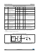
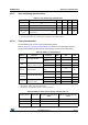
Figure 32. USB timings: definition of data signal rise and fall time
6.3.24 CAN (controller area network) interface
Refer to Section 6.3.14: I/O port characteristics for more details on the input/output alternate
function characteristics (CAN_TX and CAN_RX).
6.3.25 SDADC characteristics
ai14137
t
f
Differential
Data Lines
V
SS
V
CR S
t
r
Crossover
points
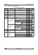
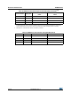
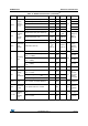
Table 73. USB: Full-speed electrical characteristics
(1)
Symbol Parameter Conditions Min Typ Max Unit
Driver characteristics
t
r
Rise time
(2)
C
L
= 50 pF
4 - 20 ns
t
f
Fall time
(2)
C
L
= 50 pF 4 - 20 ns
t
rfm
Rise/ fall time matching t
r
/t
f
90 - 110 %
V
CRS
Output signal crossover voltage - 1.3 - 2.0 V
Output driver
Impedance
(3)
Z
DRV
driving high and
low
28 40 44 Ω
1. Guaranteed by design, not tested in production.
2.
Measured from 10% to 90% of the data signal. For more detailed informations, please refer to USB Specification - Chapter
7 (version 2.0).
3. No external termination series resistors are required on USB_DP (D+) and USB_DM (D-), the matching impedance is
already included in the embedded driver.
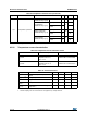
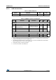
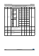
Table 74. SDADC characteristics
(1)
Symbol Parameter Conditions Min Typ Max Unit Note
V
DDSDx
Power
supply
Slow mode (f
ADC
= 1.5 MHz) 2.2 - V
DDA
V
Fast mode (f
ADC
= 6 MHz) 2.4 - V
DDA
f
ADC
SDADC
clock
frequency
Slow mode (f
ADC
= 1.5 MHz) 0.5 1.5 1.65
MHz
Fast mode (f
ADC
= 6 MHz) 0.5 6 6.3
V
REFSD+
Positive ref.
voltage
1.1 - V
DDSDx
V
V
REFSD-
Negative
ref. voltage
-V
SSA
-V