
Datasheet

DocID022691 Rev 4 101/131
STM32F37xxx Electrical characteristics
114
6.3.18 DAC electrical specifications
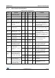
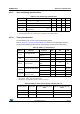
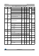
Table 63. DAC characteristics
Symbol Parameter Min Typ Max Unit Comments
V
DDA
Analog supply voltage 2.4 - 3.6 V
V
REF+
Reference supply voltage 2.4 - 3.6 V V
REF+
must always be below V
DDA
V
SSA
Ground 0 - 0 V
R
LOAD
(1)
Resistive load with buffer
ON
5- - kΩ
R
O
(1)
Impedance output with
buffer OFF
-- 15 kΩ
When the buffer is OFF, the
Minimum resistive load between
DAC_OUT and V
SS
to have a 1%
accuracy is 1.5 MΩ
C
LOAD
(1)
Capacitive load - - 50 pF
Maximum capacitive load at
DAC_OUT pin (when the buffer is
ON).
DAC_OUT
min
(1)
Lower DAC_OUT voltage
with buffer ON
0.2 - - V
It gives the maximum output
excursion of the DAC.
It corresponds to 12-bit input code
(0x0E0) to (0xF1C) at V
REF+
= 3.6 V
and (0x155) and (0xEAB) at V
REF+
= 2.4 V
DAC_OUT
max
(1)
Higher DAC_OUT voltage
with buffer ON
--V
DDA
– 0.2 V
DAC_OUT
min
(1)
Lower DAC_OUT voltage
with buffer OFF
-0.5 - mV
It gives the maximum output
excursion of the DAC.
DAC_OUT
max
(1)
Higher DAC_OUT voltage
with buffer OFF
--
V
REF+
–
1LSB
V
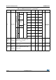
I
DDVREF+
(3
)
DAC DC current
consumption in quiescent
mode (Standby mode)
- - 220 µA
With no load, worst code (0xF1C) at
V
REF+
= 3.6 V in terms of DC
consumption on the inputs
I
DDA
(3)
DAC DC current
consumption in quiescent
mode
(2)
- - 380 µA
With no load, middle code (0x800)
on the inputs
- - 480 µA
With no load, worst code (0xF1C) at
V
REF+
= 3.6 V in terms of DC
consumption on the inputs
DNL
(3)
Differential non linearity
Difference between two
consecutive code-1LSB)
-- ±0.5 LSB
Given for the DAC in 10-bit
configuration
-- ±2 LSB
Given for the DAC in 12-bit
configuration
INL
(3)
Integral non linearity
(difference between
measured value at Code i
and the value at Code i on a
line drawn between Code 0
and last Code 1023)
-- ±1LSB
Given for the DAC in 10-bit
configuration
-- ±4LSB
Given for the DAC in 12-bit
configuration