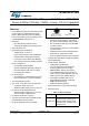
STM32F373xx ARM Cortex-M4 32b MCU+FPU, up to 256KB Flash+32KB SRAM timers, 4 ADCs (12/16-bit), 3 DACs, 2 comp., 2.0-3.6 V operation Datasheet - production data Features FBGA ® • Core: ARM 32-bit Cortex™-M4 CPU (72 MHz max), single-cycle multiplication and HW division, DSP instruction with FPU (floatingpoint unit) and MPU (memory protection unit) • 1.25 DMIPS/MHz (Dhrystone 2.
Contents STM32F37xxx Contents 1 Introduction . . . . . . . . . . . . . . . . . . . . . . . . . . . . . . . . . . . . . . . . . . . . . . . . 8 2 Description . . . . . . . . . . . . . . . . . . . . . . . . . . . . . . . . . . . . . . . . . . . . . . . . . 9 3 Functional overview . . . . . . . . . . . . . . . . . . . . . . . . . . . . . . . . . . . . . . . . 12 3.1 ARM® Cortex™-M4 core with embedded Flash and SRAM . . . . . . . . . . 12 3.2 Memory protection unit . . . . . . . . . . . . . . . . . .
STM32F37xxx Contents 3.17.2 Basic timers (TIM6, TIM7, TIM18) . . . . . . . . . . . . . . . . . . . . . . . . . . . . . 22 3.17.3 Independent watchdog (IWDG) . . . . . . . . . . . . . . . . . . . . . . . . . . . . . . . 23 3.17.4 System window watchdog (WWDG) . . . . . . . . . . . . . . . . . . . . . . . . . . . 23 3.17.5 SysTick timer . . . . . . . . . . . . . . . . . . . . . . . . . . . . . . . . . . . . . . . . . . . . . 23 3.18 Real-time clock (RTC) and backup registers . . . . . . . . . . . .
Contents 7 STM32F37xxx 6.3.7 External clock source characteristics . . . . . . . . . . . . . . . . . . . . . . . . . . . 72 6.3.8 Internal clock source characteristics . . . . . . . . . . . . . . . . . . . . . . . . . . . 77 6.3.9 PLL characteristics . . . . . . . . . . . . . . . . . . . . . . . . . . . . . . . . . . . . . . . . 78 6.3.10 Memory characteristics . . . . . . . . . . . . . . . . . . . . . . . . . . . . . . . . . . . . . 79 6.3.11 EMC characteristics . . . . . . . . . . . . . . . . .
STM32F37xxx List of tables List of tables Table 1. Table 2. Table 3. Table 4. Table 5. Table 6. Table 7. Table 8. Table 9. Table 10. Table 11. Table 12. Table 13. Table 14. Table 15. Table 16. Table 17. Table 18. Table 19. Table 20. Table 21. Table 22. Table 23. Table 24. Table 25. Table 26. Table 27. Table 28. Table 29. Table 30. Table 31. Table 32. Table 33. Table 34. Table 35. Table 36. Table 37. Table 38. Table 39. Table 40. Table 41. Table 42. Table 43. Table 44. Table 45. Table 46. Table 47.
List of tables Table 49. Table 50. Table 51. Table 52. Table 53. Table 54. Table 55. Table 56. Table 57. Table 58. Table 59. Table 60. Table 61. Table 62. Table 63. Table 64. Table 65. Table 66. Table 67. Table 68. Table 69. Table 70. Table 71. Table 72. Table 73. Table 74. Table 75. Table 76. Table 77. Table 78. Table 79. Table 80. Table 81. Table 82. 6/131 STM32F37xxx ESD absolute maximum ratings . . . . . . . . . . . . . . . . . . . . . . . . . . . . . . . . . . . . . . . . . . . . .
STM32F37xxx List of figures List of figures Figure 1. Figure 2. Figure 3. Figure 4. Figure 5. Figure 6. Figure 7. Figure 8. Figure 9. Figure 10. Figure 11. Figure 12. Figure 13. Figure 14. Figure 15. Figure 16. Figure 17. Figure 18. Figure 19. Figure 20. Figure 21. Figure 22. Figure 23. Figure 24. Figure 25. Figure 26. Figure 27. Figure 28. Figure 29. Figure 30. Figure 31. Figure 32. Figure 33. Figure 34. Figure 35. Figure 36. Figure 37. Figure 38. Figure 39. Figure 40. Block diagram . . . . . . . . . .
Introduction 1 STM32F37xxx Introduction This datasheet provides the ordering information and mechanical device characteristics of the STM32F373x microcontrollers. This STM32F373x datasheet should be read in conjunction with the STM32F373x reference manual. The reference manual is available from the STMicroelectronics website www.st.com. For information on the Cortex™-M4 with FPU core, please refer to: 8/131 • Cortex™-M4 with FPU Technical Reference Manual, available from the www.arm.
STM32F37xxx 2 Description Description The STM32F373x family is based on the high-performance ARM® Cortex™-M4 32-bit RISC core operating at a frequency of up to 72 MHz, and embedding a floating point unit (FPU), a memory protection unit (MPU) and an embedded trace macrocell (ETM). The family incorporates high-speed embedded memories (up to 256 Kbyte of Flash memory, up to 32 Kbytes of SRAM), and an extensive range of enhanced I/Os and peripherals connected to two APB buses.
Description STM32F37xxx Table 2. Device overview STM32F 373Cx Peripheral STM32F 373Rx Flash (Kbytes) 64 128 256 64 128 256 64 128 256 SRAM (Kbytes) 16 24 32 16 24 32 16 24 32 Timers General purpose 9 (16-bit) 2 (32 bit) Basic 3 (16-bit) SPI/I2S 3 2 Comm.
STM32F37xxx Description Figure 1.
Functional overview STM32F37xxx 3 Functional overview 3.1 ARM® Cortex™-M4 core with embedded Flash and SRAM The ARM Cortex-M4 processor is the latest generation of ARM processors for embedded systems. It was developed to provide a low-cost platform that meets the needs of MCU implementation, with a reduced pin count and low-power consumption, while delivering outstanding computational performance and an advanced response to interrupts.
STM32F37xxx 3.3 Functional overview Embedded Flash memory All STM32F373x devices feature up to 256 Kbytes of embedded Flash memory available for storing programs and data. The Flash memory access time is adjusted to the CPU clock frequency (0 wait state from 0 to 24 MHz, 1 wait state from 24 to 48 MHz and 2 wait states above). 3.
Functional overview STM32F37xxx 3.7 Power management 3.7.1 Power supply schemes 3.7.2 • VDD: external power supply for I/Os and the internal regulator. It is provided externally through VDD pins, and can be 2.0 to 3.6 V. • VDDA = 2.0 to 3.6 V: – external analog power supplies for Reset blocks, RCs and PLL – supply voltage for 12-bit ADC, DACs and comparators (minimum voltage to be applied to VDDA is 2.4 V when the 12-bit ADC and DAC are used). • VDDSD12 and VDDSD3 = 2.2 to 3.
STM32F37xxx 3.7.4 Functional overview Low-power modes The STM32F373x supports three low-power modes to achieve the best compromise between low power consumption, short startup time and available wakeup sources: • Sleep mode In Sleep mode, only the CPU is stopped. All peripherals continue to operate and can wake up the CPU when an interrupt/event occurs. • Stop mode Stop mode achieves the lowest power consumption while retaining the content of SRAM and registers. All clocks in the 1.
Functional overview STM32F37xxx Do not reconfigure GPIO pins which are not present on 48 and 64 pin packages to the analog mode. Additional current consumption in the range of tens of µA per pin can be observed if VDDA is higher than VDDIO. 3.10 Direct memory access (DMA) The flexible 12-channel, general-purpose DMA is able to manage memory-to-memory, peripheral-to-memory and memory-to-peripheral transfers.
STM32F37xxx 3.12 Functional overview 12-bit analog-to-digital converter (ADC) The 12-bit analog-to-digital converter is based on a successive approximation register (SAR) architecture. It has up to 16 external channels (AIN15:0) and 3 internal channels (temperature sensor, voltage reference, VBAT voltage measurement) performing conversions in single-shot or scan modes. In scan mode, automatic conversion is performed on a selected group of analog inputs. The ADC can be served by the DMA controller.
Functional overview 3.13 STM32F37xxx 16-bit sigma delta analog-to-digital converters (SDADC) Up to three 16-bit sigma-delta analog-to-digital converters are embedded in the STM32F373x. They have up to two separate supply voltages allowing the analog function voltage range to be independent from the STM32F373x power supply. They share up to 21 input pins which may be configured in any combination of single-ended (up to 21) or differential inputs (up to 11). The conversion speed is up to 16.
STM32F37xxx 3.15 Functional overview Fast comparators (COMP) The STM32F373x embeds up to 2 comparators with rail-to-rail inputs and high-speed output. The reference voltage can be internal or external (delivered by an I/O). The threshold can be one of the following: • DACs channel outputs • External I/O • Internal reference voltage (VREFINT) or submultiple (1/4 VREFINT, 1/2 VREFINT and 3/4 VREFINT) The comparators can be combined into a window comparator.
Functional overview STM32F37xxx Table 3. Capacitive sensing GPIOs available on STM32F373x devices (continued) Group 3 4 Capacitive sensing signal name Pin name Capacitive sensing signal name Pin name TSC_G3_IO1 PC4 TSC_G7_IO1 PE2 TSC_G3_IO2 PC5 TSC_G7_IO2 PE3 TSC_G3_IO3 PB0 TSC_G7_IO3 PE4 TSC_G3_IO4 PB1 TSC_G7_IO4 PE5 TSC_G4_IO1 PA9 TSC_G8_IO1 PD12 TSC_G4_IO2 PA10 TSC_G8_IO2 PD13 TSC_G4_IO3 PA13 TSC_G8_IO3 PD14 TSC_G4_IO4 PA14 TSC_G8_IO4 PD15 Group 7 8 Table 4.
STM32F37xxx 3.17 Functional overview Timers and watchdogs The STM32F373x includes two 32-bit and nine 16-bit general-purpose timers, three basic timers, two watchdog timers and a SysTick timer. The table below compares the features of the advanced control, general purpose and basic timers. Table 5.
Functional overview 3.17.1 STM32F37xxx General-purpose timers (TIM2 to TIM5, TIM12 to TIM17, TIM19) There are eleven synchronizable general-purpose timers embedded in the STM32F373x (see Table 5 for differences). Each general-purpose timer can be used to generate PWM outputs, or act as a simple time base.
STM32F37xxx 3.17.3 Functional overview Independent watchdog (IWDG) The independent watchdog is based on a 12-bit downcounter and 8-bit prescaler. It is clocked from an independent 40 kHz internal RC and as it operates independently from the main clock, it can operate in Stop and Standby modes. It can be used either as a watchdog to reset the device when a problem occurs, or as a free running timer for application timeout management. It is hardware or software configurable through the option bytes.
Functional overview STM32F37xxx The RTC is an independent BCD timer/counter. Its main features are the following: • Calendar with subsecond, seconds, minutes, hours (12 or 24 format), week day, date, month, year, in BCD (binary-coded decimal) format. • Automatic correction for 28th, 29th (leap year), 30th and 31st day of the month. • 2 programmable alarms with wake up from Stop and Standby mode capability. • Periodic wakeup unit with programmable resolution and period.
STM32F37xxx Functional overview ALERT protocol management. They also have a clock domain independent from the CPU clock, allowing the application to wake up the MCU from Stop mode on address match. The I2C interfaces can be served by the DMA controller Refer to Table 7 for the differences between I2C1 and I2C2. Table 7.
Functional overview STM32F37xxx Table 8. STM32F373x USART implementation (continued) USART modes/features(1) USART1 USART2 USART3 Dual clock domain and wakeup from Stop mode X X X Receiver timeout interrupt X X X Modbus communication X X X Auto baud rate detection X X X Driver Enable X X X 1. X = supported. 3.
STM32F37xxx 3.22 Functional overview High-definition multimedia interface (HDMI) - consumer electronics control (CEC) The device embeds a HDMI-CEC controller that provides hardware support for the Consumer Electronics Control (CEC) protocol (Supplement 1 to the HDMI standard). This protocol provides high-level control functions between all audiovisual products in an environment. It is specified to operate at low speeds with minimum processing and memory overhead.
Functional overview 3.26 STM32F37xxx Embedded trace macrocell™ The ARM embedded trace macrocell provides a greater visibility of the instruction and data flow inside the CPU core by streaming compressed data at a very high rate from the STM32F373x through a small number of ETM pins to an external hardware trace port analyzer (TPA) device. The TPA is connected to a host computer using USB, Ethernet, or any other high-speed channel.
STM32F37xxx 4 Pinouts and pin description Pinouts and pin description VDD_1 VSS_1 PB9 PB8 BOOT0 PB7 PB6 PB5 PB4 PB3 PA15 PA14 Figure 2.
Pinouts and pin description STM32F37xxx VDD_1 VSS_1 PB9 PB8 BOOT0 PB7 PB6 PB5 PB4 PB3 PD2 PC12 PC11 PC10 PA15 PA14 Figure 3.
STM32F37xxx Pinouts and pin description 100 99 98 97 96 95 94 93 92 91 90 89 88 87 86 85 84 83 82 81 80 79 78 77 76 VDD_1 VSS_1 PE1 PE0 PB9 PB8 BOOT0 PB7 PB6 PB5 PB4 PB3 PD7 PD6 PD5 PD4 PD3 PD2 PD1 PD0 PC12 PC11 PC10 PA15 PA14 Figure 4.
Pinouts and pin description STM32F37xxx Figure 5.
STM32F37xxx Pinouts and pin description Table 10. Legend/abbreviations used in the pinout table Name Pin name Abbreviation Unless otherwise specified in brackets below the pin name, the pin function during and after reset is the same as the actual pin name Pin type I/O structure Notes Definition S Supply pin I Input only pin I/O Input / output pin FT 5 V tolerant I/O FTf 5 V tolerant I/O, FM+ capable TTa 3.3 V tolerant I/O directly connected to ADC TC Standard 3.
Pinouts and pin description STM32F37xxx Table 11.
STM32F37xxx Pinouts and pin description Table 11.
Pinouts and pin description STM32F37xxx Table 11.
STM32F37xxx Pinouts and pin description Table 11.
Pinouts and pin description STM32F37xxx Table 11.
STM32F37xxx Pinouts and pin description Table 11.
Pinouts and pin description STM32F37xxx Table 11.
Pin Name AF0 AF1 AF2 AF3 AF4 AF5 AF6 AF7 AF8 USART2_CTS COMP1 _OUT TIM2_ CH1_ ETR TIM5_ TSC_ CH1_ G1_IO1 ETR TIM2_ CH2 TIM5_ TSC_ CH2 G1_IO2 SPI3_SCK/ I2S3_CK PA2 TIM2_ CH3 TIM5_ TSC_ CH3 G1_IO3 SPI3_MISO/ USART2_TX I2S3_MCK PA3 TIM2_ CH4 TIM5_ TSC_ CH4 G1_IO4 SPI3_MOSI /I2S3_SD USART2_RX SPI3_NSS/ I2S3_WS USART2_CK PA0 PA1 RTC_ REFIN DocID022691 Rev 4 PA4 TIM3_ TSC_ CH2 G2_IO1 SPI1_NSS/ I2S1_WS TSC_ G2_IO2 SPI1_SCK/ I2S1_CK USART2_RTS AF9 AF10 AF11 AF14 AF15 TIM19
Pin Name AF0 AF1 PA13 SWDIO TIM16_ -JTMS CH1N PA14 SWCLK -JTCK PA15 JTDI AF2 AF3 AF4 TIM5_ TSC_ CH4 G4_IO3 AF5 IR-OUT AF6 AF7 SPI1_MISO /I2S1_MCK USART3_CTS TSC_ I2C1_ G4_IO4 SDA TIM2_ CH1_ETR TSC_ SYNC I2C1_ SCL SPI1_NSS/ I2S1_WS SPI3_NSS/ I2S3_WS AF8 AF9 AF10 AF11 AF14 AF15 TIM4_ CH3 EVENT OUT TIM12 _CH1 EVENT OUT TIM12 _CH2 EVENT OUT STM32F37xxx Table 12.
Pin Name AF0 AF1 AF2 AF3 PB0 TIM3_CH3 TSC_ G3_IO3 PB1 TIM3_CH4 TSC_ G3_IO4 AF4 AF5 AF6 AF7 AF8 AF9 SPI_MOSI/ I2S1_SD AF10 TIM3_ CH2 AF11 AF15 EVENTOUT EVENTOUT PB2 EVENTOUT PB3 JTDOTIM2_ TRACESWO CH2 PB4 NJTRST TIM4_ETR TSC_ G5_IO1 SPI1_SCK/ I2S1_CK TIM16_ TSC_ TIM3_CH1 CH1 G5_IO2 SPI3_SCK/ I2S3_CK USART2_TX TIM13_ TIM3_ CH1 ETR EVENTOUT SPI1_MISO SPI3_MISO/ USART2_RX /I2S1_MCK I2S3_MCK TIM15_ TIM17 CH1N _BKIN EVENTOUT DocID022691 Rev 4 PB5 TIM16_ TIM3_CH2 BKIN I2C1_
Pin Name AF0 AF1 AF2 AF3 AF4 AF5 AF6 AF7 DocID022691 Rev 4 PC0 EVENTOUT TIM5_CH1_ETR PC1 EVENTOUT TIM5_CH2 PC2 EVENTOUT TIM5_CH3 SPI2_MISO/I2S2_MCK PC3 EVENTOUT TIM5_CH4 SPI2_MOSI/I2S2_SD PC4 EVENTOUT TIM13_CH1 PC5 EVENTOUT PC6 EVENTOUT TIM3_CH1 SPI1_NSS/I2S1_WS PC7 EVENTOUT TIM3_CH2 SPI1_SCK/I2S1_CK PC8 EVENTOUT TIM3_CH3 SPI1_MISO/I2S1_MCK PC9 EVENTOUT TIM3_CH4 SPI1_MOSI/I2S1_SD PC10 EVENTOUT TIM19_CH1 SPI3_SCK/I2S3_CK USART3_TX PC11 EVENTOUT TIM19_CH2 S
Pin Name AF0 AF1 AF2 AF3 AF4 AF5 AF6 AF7 DocID022691 Rev 4 PD0 EVENTOUT TIM19_CH4 CAN_RX PD1 EVENTOUT TIM19_ETR CAN_TX PD2 EVENTOUT TIM3_ETR PD3 EVENTOUT SPI2_MISO/I2S2_MCK USART2_CTS PD4 EVENTOUT SPI2_MOSI/I2S2_SD USART2_RTS PD5 EVENTOUT PD6 EVENTOUT SPI2_NSS/I2S2_WS USART2_RX PD7 EVENTOUT SPI2_SCK/I2S2_CK USART2_CK PD8 EVENTOUT TSC_G6_IO3 SPI2_SCK/I2S2_CK USART3_TX PD9 EVENTOUT TSC_G6_IO4 PD10 EVENTOUT USART3_CK PD11 EVENTOUT USART3_CTS PD12 EVENTOUT
Pin Name AF0 AF1 PE0 EVENTOUT PE1 EVENTOUT AF2 AF3 TIM4_ETR EVENTOUT TSC_G7_IO1 PE3 TRACED0 EVENTOUT TSC_G7_IO2 PE4 TRACED1 EVENTOUT TSC_G7_IO3 PE5 TRACED2 EVENTOUT TSC_G7_IO4 PE6 TRACED3 EVENTOUT DocID022691 Rev 4 PE8 EVENTOUT PE9 EVENTOUT PE10 EVENTOUT PE11 EVENTOUT PE12 EVENTOUT PE13 EVENTOUT PE14 EVENTOUT PE15 EVENTOUT AF6 AF7 USART1_RX TRACECLK EVENTOUT AF5 USART1_TX PE2 PE7 AF4 STM32F37xxx Table 16.
Pin Name AF0 AF1 AF2 AF3 AF4 PF0 I2C2_SDA PF1 I2C2_SCL PF2 EVENTOUT PF4 EVENTOUT PF6 EVENTOUT PF7 EVENTOUT PF9 EVENTOUT PF10 EVENTOUT AF5 AF6 AF7 I2C2_SMBA TIM4_CH4 I2C2_SCL I2C2_SDA SPI1_MOSI/I2S1_SD USART3_RTS USART2_CK Pinouts and pin description 47/131 Table 17.
Memory mapping 5 STM32F37xxx Memory mapping Figure 6.
STM32F37xxx Memory mapping Table 18.
Memory mapping STM32F37xxx Table 18.
STM32F37xxx Memory mapping Table 18.
Electrical characteristics STM32F37xxx 6 Electrical characteristics 6.1 Parameter conditions Unless otherwise specified, all voltages are referenced to VSS. 6.1.1 Minimum and maximum values Unless otherwise specified, the minimum and maximum values are guaranteed in the worst conditions of ambient temperature, supply voltage and frequencies by tests in production on 100% of the devices with an ambient temperature at TA = 25 °C and TA = TAmax (given by the selected temperature range).
STM32F37xxx Power supply scheme Figure 9. Power supply scheme VBAT Backup circuitry (LSE,RTC, Wakeup logic Backup registers) Level shifter Po wer swi tch 1.65 - 3.6 V OUT GP I/Os @VDD IN IO Logic VDD 3 × VDD 2 × 100 nF + 1 × 4.7 μF Regulator 1.8 V Kernel logic (CPU, Digital & Memories) OUT GP I/Os @VDDSD3 IN OUT GP I/Os @VDDSD12 VDDSD12 IN Level shifter 2 × VSS IO Logic Level shifter 6.1.
Electrical characteristics STM32F37xxx Caution: Each power supply pair (VDD/VSS, VDDA/VSSA etc..) must be decoupled with filtering ceramic capacitors as shown above. These capacitors must be placed as close as possible to, or below, the appropriate pins on the underside of the PCB to ensure the good functionality of the device. 6.1.7 Current consumption measurement Figure 10.
STM32F37xxx 6.2 Electrical characteristics Absolute maximum ratings Stresses above the absolute maximum ratings listed in Table 19: Voltage characteristics, Table 20: Current characteristics, and Table 21: Thermal characteristics may cause permanent damage to the device. These are stress ratings only and functional operation of the device at these conditions is not implied. Exposure to maximum rating conditions for extended periods may affect device reliability. Table 19.
Electrical characteristics STM32F37xxx Depending on the SDADCx operation mode, there can be more constraints between VREFSD+, VDDSD12 and VDDSD3 which are described in reference manual RM0313. Table 20. Current characteristics Symbol Ratings Max.
STM32F37xxx Electrical characteristics 6.3 Operating conditions 6.3.1 General operating conditions Table 22. General operating conditions Symbol Parameter Conditions Min Max Unit fHCLK Internal AHB clock frequency 0 72 fPCLK1 Internal APB1 clock frequency 0 36 fPCLK2 Internal APB2 clock frequency 0 72 2.0 3.6 2.4 3.6 2.0 3.6 2.2 3.6 2.0 3.6 2.2 3.6 2.0 3.6 2.4 3.6 2.0 3.6 1.1 3.6 V Backup operating voltage 1.65 3.6 V Input voltage on FT and FTf pins(2) - 0.
Electrical characteristics STM32F37xxx Table 22.
STM32F37xxx 6.3.3 Electrical characteristics Embedded reset and power control block characteristics The parameters given in Table 24 are derived from tests performed under ambient temperature and VDD supply voltage conditions summarized in Table 22. Table 24. Embedded reset and power control block characteristics Symbol Parameter VPOR/PDR(1) VPDRhyst (3) tRSTTEMPO (3) Power on/power down reset threshold Conditions Min Falling edge Rising edge Typ Max Unit 1.80(2) 1.88 1.96 V 1.84 1.
Electrical characteristics 6.3.4 STM32F37xxx Embedded reference voltage The parameters given in Table 27 are derived from tests performed under ambient temperature and VDD supply voltage conditions summarized in Table 22. Table 26. Embedded internal reference voltage calibration values Calibration value name Description Raw data acquired at temperature of 30 °C VDDA= 3.3 V VREFINT_CAL Memory address 0x1FFF F7BA - 0x1FFF F7BB Table 27.
STM32F37xxx 6.3.5 Electrical characteristics Supply current characteristics The current consumption is a function of several parameters and factors such as the operating voltage, ambient temperature, I/O pin loading, device software configuration, operating frequencies, I/O pin switching rate, program location in memory and executed binary code. The current consumption is measured as described in Figure 10: Current consumption measurement scheme.
Electrical characteristics STM32F37xxx Table 28. Typical and maximum current consumption from VDD supply at VDD = 3.6 V (continued) All peripherals enabled Symbol Parameter Conditions fHCLK Max @ TA(1) Typ 25 °C 72 MHz HSE bypass, PLL on Supply current in Run mode, code executing from RAM HSE bypass, PLL off HSI clock, PLL on HSI clock, PLL off IDD HSE bypass, PLL on Supply current in Sleep mode, code executing from Flash or RAM HSE bypass, PLL off HSI clock, PLL on HSI clock, PLL off 63.
STM32F37xxx Electrical characteristics Table 29. Typical and maximum current consumption from VDDA supply VDDA= 2.
Electrical characteristics STM32F37xxx Table 31. Typical and maximum VDDA consumption in Stop and Standby modes Parameter Supply current in Stop mode IDDA Supply current in Standby mode Max(1) 2.0 V 2.4 V 2.7 V 3.0 V 3.3 V 3.6 V TA= TA= TA= 25 °C 85 °C 105 °C Conditions VDDA and VDDSD12 Symbol Typ@VDD (VDD=VDDA) Regulator in run mode, all 1.99 oscillators OFF 2.07 2.19 2.33 2.46 2.64 10.8 11.8 12.4 Regulator in low-power 1.99 mode, all oscillators OFF 2.07 2.18 2.32 2.47 2.63 10.
STM32F37xxx Electrical characteristics Figure 11. Typical VBAT current consumption (LSE and RTC ON/LSEDRV[1:0]='00') 1.6 1.4 1.65 V I VBAT (μA) 1.2 1.8 V 1 2V 2.4 V 0.8 2.7 V 0.6 3V 0.4 3.3 V 0.2 3.6 V 0 25°C 60°C 85°C 105°C TA (°C) MS31413V1 Typical current consumption The MCU is placed under the following conditions: • VDD = VDDA = VDDSD12 = VDDSD3 = 3.
Electrical characteristics STM32F37xxx Table 33.
STM32F37xxx Electrical characteristics Table 34.
Electrical characteristics STM32F37xxx I/O system current consumption The current consumption of the I/O system has two components: static and dynamic. I/O static current consumption All the I/Os used as inputs with pull-up generate current consumption when the pin is externally held low. The value of this current consumption can be simply computed by using the pull-up/pull-down resistors values given in Table 52: I/O static characteristics.
STM32F37xxx Electrical characteristics Table 35. Switching output I/O current consumption Symbol Parameter Conditions(1) VDD = 3.3 V Cext = 0 pF C = CINT + CEXT+ CS VDD = 3.3 V Cext = 10 pF C = CINT + CEXT+ CS ISW I/O current consumption VDD = 3.3 V Cext = 22 pF C = CINT + CEXT+ CS VDD = 3.3 V Cext = 33 pF C = CINT + CEXT+ CS VDD = 3.3 V Cext = 47 pF C = CINT + CEXT+ CS I/O toggling frequency (fSW) Typ 2 MHz 0.77 4 MHz 0.87 8 MHz 0.95 18 MHz 1.59 36 MHz 2.57 48 MHz 3.11 2 MHz 0.
Electrical characteristics STM32F37xxx On-chip peripheral current consumption The MCU is placed under the following conditions: • All I/O pins are in analog input configuration. • All peripherals are disabled unless otherwise mentioned. • The given value is calculated by measuring the current consumption • – with all peripherals clocked off; – with only one peripheral clocked on. Ambient operating temperature at 25°C and VDD = VDDA= 3.3 Volts. Table 36.
STM32F37xxx Electrical characteristics Table 36. Peripheral current consumption (continued) Typical consumption(1) Peripheral Unit APB1 peripherals APB1-Bridge(3) 6.9 TIM2 47.9 TIM3 36.8 TIM4 36.9 TIM5 45.5 TIM6 8.4 TIM7 8.2 TIM12 21.3 TIM13 14.2 TIM14 14.4 TIM18 10.1 WWDG 4.7 SPI2 24.3 SPI3 25.3 USART2 45.3 USART3 43.1 I2C1 14.0 I2C2 13.9 USB 27.9 CAN 38.1 DAC2 7.7 PWR 5.4 DAC1 14.8 CEC 5.4 µA/MHz 1.
Electrical characteristics STM32F37xxx All timings are derived from tests performed under ambient temperature and VDD supply voltage conditions summarized in Table 22. Table 37. Low-power mode wakeup timings Symbol Parameter Typ @VDD = VDDA Conditions = 2.0 V = 2.4 V = 2.7 V tWUSTOP tWUSTANDB Y tWUSLEEP 6.3.7 Wakeup from Stop mode Wakeup from Standby mode Max =3V = 3.3 V Regulator in run mode 4.1 3.9 3.8 3.7 3.6 4.5 Regulator in low power mode 7.9 6.7 6.1 5.7 5.4 8.
STM32F37xxx Electrical characteristics Figure 12. High-speed external clock source AC timing diagram tW(HSEH) VHSEH 90% VHSEL 10% tr(HSE) tf(HSE) t tW(HSEL) THSE MS19214V2 Low-speed external user clock generated from an external source In bypass mode the LSE oscillator is switched off and the input pin is a standard GPIO. The external clock signal has to respect the I/O characteristics in Section 6.3.14. However, the recommended clock input waveform is shown in Figure 13. Table 39.
Electrical characteristics STM32F37xxx Figure 13. Low-speed external clock source AC timing diagram tW(LSEH) VLSEH 90% 10% VLSEL tr(LSE) t tf(LSE) tW(LSEL) TLSE MS19215V2 High-speed external clock generated from a crystal/ceramic resonator The high-speed external (HSE) clock can be supplied with a 4 to 32 MHz crystal/ceramic resonator oscillator. All the information given in this paragraph are based on design simulation results obtained with typical external components specified in Table 40.
STM32F37xxx Electrical characteristics For CL1 and CL2, it is recommended to use high-quality external ceramic capacitors in the 5 pF to 20 pF range (typ.), designed for high-frequency applications, and selected to match the requirements of the crystal or resonator (see Figure 14). CL1 and CL2 are usually the same size. The crystal manufacturer typically specifies a load capacitance which is the series combination of CL1 and CL2.
Electrical characteristics STM32F37xxx Low-speed external clock generated from a crystal resonator The low-speed external (LSE) clock can be supplied with a 32.768 kHz crystal resonator oscillator. All the information given in this paragraph are based on design simulation results obtained with typical external components specified in Table 41.
STM32F37xxx Electrical characteristics Figure 15. Typical application with a 32.768 kHz crystal Resonator with integrated capacitors CL1 fLSE OSC32_IN Drive programmable amplifier 32.768 kH z resonator OSC32_OU T CL2 MS30253V1 Note: An external resistor is not required between OSC32_IN and OSC32_OUT and it is forbidden to add one. 6.3.
Electrical characteristics STM32F37xxx Figure 16. HSI oscillator accuracy characterization results ACCHSI 5% 4% 3% 2% MAX 1% MIN 0% -40 TA [°C] -20 0 20 40 60 80 100 120 - 1% - 2% - 3% -4% -5% MS30986V2 Low-speed internal (LSI) RC oscillator Table 43. LSI oscillator characteristics(1) Symbol fLSI tsu(LSI) Parameter Min Typ Max Unit 30 40 60 kHz LSI oscillator startup time - - 85 µs LSI oscillator power consumption - 0.75 1.2 µA Frequency (2) IDD(LSI)(2) 1. VDDA = 3.
STM32F37xxx 6.3.10 Electrical characteristics Memory characteristics Flash memory The characteristics are given at TA = –40 to 105 °C unless otherwise specified. Table 45. Flash memory characteristics Min Typ Max(1) Unit 16-bit programming time TA = –40 to +105 °C 40 53.
Electrical characteristics 6.3.11 STM32F37xxx EMC characteristics Susceptibility tests are performed on a sample basis during device characterization. Functional EMS (electromagnetic susceptibility) While a simple application is executed on the device (toggling 2 LEDs through I/O ports). the device is stressed by two electromagnetic events until a failure occurs.
STM32F37xxx Electrical characteristics To complete these trials, ESD stress can be applied directly on the device, over the range of specification values. When unexpected behavior is detected, the software can be hardened to prevent unrecoverable errors occurring (see application note AN1015). Electromagnetic Interference (EMI) The electromagnetic field emitted by the device are monitored while a simple application is executed (toggling 2 LEDs through the I/O ports).
Electrical characteristics STM32F37xxx Static latch-up Two complementary static tests are required on six parts to assess the latch-up performance: • A supply overvoltage is applied to each power supply pin • A current injection is applied to each input, output and configurable I/O pin These tests are compliant with EIA/JESD 78A IC latch-up standard. Table 50. Electrical sensitivities Symbol LU 6.3.
STM32F37xxx Electrical characteristics Table 51.
Electrical characteristics 6.3.14 STM32F37xxx I/O port characteristics General input/output characteristics Unless otherwise specified, the parameters given in Table 52 are derived from tests performed under the conditions summarized in Table 22. All I/Os are CMOS and TTL compliant. Table 52. I/O static characteristics (1) Symbol VIL Parameter Low level input voltage Conditions High level input voltage Vhys Ilkg Input leakage current (3) Max Unit (2) - - 0.3VDD+0.
STM32F37xxx Note: Electrical characteristics I/O pins are powered from VDD voltage except pins which can be used as SDADC inputs: - The PB2, PB10 and PE7 to PE15 I/O pins are powered from VDDSD12. - PB14 to PB15 and PD8 to PD15 I/O pins are powered from VDDSD3. All I/O pin ground is internally connected to VSS. VDD mentioned in the Table 52 represents power voltage for a given I/O pin (VDD or VDDSD12 or VDDSD3). All I/Os are CMOS and TTL compliant (no software configuration required).
Electrical characteristics STM32F37xxx Figure 19. Five volt tolerant (FT and FTf) I/O input characteristics - CMOS port VIL/VIH (V) in = ts V IHm ndard men quire 0.7V DD re ons 0.2 V DD+ simulati n = 0.5 V IHmin on desig d Base -0.2 lations u 5V DD 0.47 ign sim x= s a e m d V IL d on e s a B S sta CMO 2.0 Area not determined 1.0 nts ard requireme CMOS stand VILmax = 0.3VDD 0.5 VDD (V) 2.7 2.0 3.6 MS30257V3 Figure 20.
STM32F37xxx Electrical characteristics Output voltage levels Unless otherwise specified, the parameters given in Table 53 are derived from tests performed under ambient temperature and VDD supply voltage conditions summarized in Table 22. All I/Os are CMOS and TTL compliant (FT, TTa or TC unless otherwise specified). Table 53.
Electrical characteristics STM32F37xxx Input/output AC characteristics The definition and values of input/output AC characteristics are given in Figure 21 and Table 54, respectively. Unless otherwise specified, the parameters given are derived from tests performed under ambient temperature and VDD supply voltage conditions summarized in Table 22. Table 54.
STM32F37xxx Electrical characteristics Figure 21. I/O AC characteristics definition 90% 10% 50% 50% 10% EXTERNAL OUTPUT ON 50 pF 90% t f(IO)out t r(IO)out T Maximum frequency is achieved if (t r + t f (≤ 2/3)T and if the duty cycle is (45-55%) when loaded by 50 pF MS32132V1 6.3.15 NRST characteristics NRST pin characteristics The NRST pin input driver uses CMOS technology. It is connected to a permanent pull-up resistor, RPU (see Table 52).
Electrical characteristics STM32F37xxx Figure 22. Recommended NRST pin protection VDD External reset circuit(1) NRST(2) R PU Internal Reset Filter 0.1 μF MS19878V1 1. The reset network protects the device against parasitic resets. 2. The user must ensure that the level on the NRST pin can go below the VIL(NRST) max level specified in Table 55. Otherwise the reset will not be taken into account by the device.
STM32F37xxx 6.3.16 Electrical characteristics Communications interfaces I2C interface characteristics The I2C interface meets the requirements of the standard I2C communication protocol with the following restrictions: the I/O pins SDA and SCL are mapped to are not “true” opendrain. When configured as open-drain, the PMOS connected between the I/O pin and VDD is disabled, but is still present. The I2C characteristics are described in Table 56. Refer also to Section 6.3.
Electrical characteristics STM32F37xxx Table 57. I2C analog filter characteristics(1) Symbol Parameter Pulse width of spikes that are suppressed by the analog filter tSP Min Max Unit 50 260 ns 1. Guaranteed by design, not tested in production. Figure 23.
STM32F37xxx Electrical characteristics SPI/I2S characteristics Unless otherwise specified, the parameters given in Table 58 for SPI or in Table 59 for I2S are derived from tests performed under ambient temperature, fPCLKx frequency and VDD supply voltage conditions summarized in Table 22. Refer to Section 6.3.14: I/O port characteristics for more details on the input/output alternate function characteristics (NSS, SCK, MOSI, MISO for SPI and WS, CK, SD for I2S). Table 58.
Electrical characteristics STM32F37xxx Figure 24. SPI timing diagram - slave mode and CPHA = 0 NSS input tc(SCK) th(NSS) tSU(NSS) SCK Input CPHA= 0 CPOL=0 tw(SCKH) tw(SCKL) CPHA= 0 CPOL=1 tv(SO) ta(SO) MISO OUT P UT tr(SCK) tf(SCK) th(SO) MS B O UT BI T6 OUT tdis(SO) LSB OUT tsu(SI) MOSI I NPUT M SB IN LSB IN B I T1 IN th(SI) ai14134c Figure 25.
STM32F37xxx Electrical characteristics Figure 26. SPI timing diagram - master mode(1) High NSS input SCK Output CPHA= 0 CPOL=0 SCK Output tc(SCK) CPHA=1 CPOL=0 CPHA= 0 CPOL=1 CPHA=1 CPOL=1 tsu(MI) MISO INP UT tw(SCKH) tw(SCKL) tr(SCK) tf(SCK) MS BIN BI T6 IN LSB IN th(MI) MOSI OUTPUT M SB OUT tv(MO) B I T1 OUT LSB OUT th(MO) ai14136V2 1. Measurement points are done at 0.5VDD level and with external CL = 30 pF.
Electrical characteristics STM32F37xxx Table 59. I2S characteristics Symbol Parameter Conditions Min Max Unit 30 70 % 1.528 1.539 Slave mode 0 12.
STM32F37xxx Electrical characteristics Figure 27. I2S slave timing diagram (Philips protocol)(1) CK Input tc(CK) CPOL = 0 CPOL = 1 tw(CKH) th(WS) tw(CKL) WS input tv(SD_ST) tsu(WS) SDtransmit LSB transmit(2) MSB transmit Bitn transmit tsu(SD_SR) LSB receive(2) SDreceive th(SD_ST) LSB transmit th(SD_SR) MSB receive Bitn receive LSB receive ai14881b 1. Measurement points are done at 0.5 VDD level and with external CL = 30 pF. 2. LSB transmit/receive of the previously transmitted byte.
Electrical characteristics 6.3.17 STM32F37xxx 12-bit ADC characteristics Unless otherwise specified, the parameters given in Table 60 are preliminary values derived from tests performed under ambient temperature, fPCLK2 frequency and VDDA supply voltage conditions summarized in Table 22. Note: It is recommended to perform a calibration after each power-up. Table 60. ADC characteristics Symbol Parameter Conditions Min Typ Max Unit VDDA Power supply 2.4 - 3.
STM32F37xxx Electrical characteristics Equation 1: RSRC max formula TS - – R ADC R SRC < ------------------------------------------------------------N+2 f ADC × C ADC × ln ( 2 ) The formula above (Equation 1) is used to determine the maximum external signal source impedance allowed for an error below 1/4 of LSB. Here N = 12 (from 12-bit resolution). Table 61. RSRC max for fADC = 14 MHz(1) Ts (cycles) tS (µs) RSRC max (kΩ) 1.5 0.11 0.4 7.5 0.54 5.9 13.5 0.96 11.4 28.5 2.04 25.2 41.5 2.
Electrical characteristics STM32F37xxx 2. ADC accuracy vs. negative injection current: Injecting a negative current on any analog input pins should be avoided as this significantly reduces the accuracy of the conversion being performed on another analog input. It is recommended to add a Schottky diode (pin to ground) to analog pins which may potentially inject negative currents. Any positive injection current within the limits specified for IINJ(PIN) and ΣIINJ(PIN) in Section 6.3.
STM32F37xxx 6.3.18 Electrical characteristics DAC electrical specifications Table 63. DAC characteristics Symbol Parameter Min Typ Max Unit Comments VDDA Analog supply voltage 2.4 - 3.6 V VREF+ Reference supply voltage 2.4 - 3.6 V VSSA Ground 0 - 0 V RLOAD(1) Resistive load with buffer ON 5 - - kΩ RO(1) Impedance output with buffer OFF - - 15 kΩ When the buffer is OFF, the Minimum resistive load between DAC_OUT and VSS to have a 1% accuracy is 1.
Electrical characteristics STM32F37xxx Table 63. DAC characteristics (continued) Symbol Offset(3) Parameter Offset error (difference between measured value at Code (0x800) and the ideal value = VREF+/2) Min Typ Max Unit Comments - - ±10 mV - - ±3 LSB Given for the DAC in 10-bit at VREF+ = 3.6 V - - ±12 LSB Given for the DAC in 12-bit at VREF+ = 3.6 V Gain error(3) Gain error - - ±0.
STM32F37xxx 6.3.19 Electrical characteristics Comparator characteristics Table 64. Comparator characteristics Symbol VDDA Parameter Conditions Min Typ Max(1) Unit Analog supply voltage 2 - 3.6 VIN Comparator input voltage range 0 - VDDA VBG Scaler input voltage - 1.2 - VSC Scaler offset voltage - ±5 ±10 mV tS_SC Scaler startup time from power down - - 0.
Electrical characteristics STM32F37xxx Table 64. Comparator characteristics (continued) Symbol Parameter Min Typ Max(1) Conditions No hysteresis (COMPxHYST[1:0]=00) Low hysteresis (COMPxHYST[1:0]=01) Vhys Comparator hysteresis Medium hysteresis (COMPxHYST[1:0]=10) High hysteresis (COMPxHYST[1:0]=11) High speed mode 3 All other power modes 5 High speed mode 7 All other power modes 9 High speed mode 18 All other power modes 19 0 Unit 13 8 10 mV 26 15 19 49 31 40 1.
STM32F37xxx 6.3.21 Electrical characteristics VBAT monitoring characteristics Table 67. VBAT monitoring characteristics Symbol Parameter Min Typ Max Unit KΩ R Resistor bridge for VBAT - 50 - Q Ratio on VBAT measurement - 2 - Error on Q -1 - +1 % ADC sampling time when reading the VBAT 1mV accuracy 5 - - µs Er (1) TS_vbat(2) 1. Guaranteed by design, not tested in production. 2. Shortest sampling time can be determined in the application by multiple iterations. 6.3.
Electrical characteristics STM32F37xxx Table 69. IWDG min/max timeout period at 40 kHz (LSI) (continued)(1)(2) Prescaler divider PR[2:0] bits Min timeout (ms) RL[11:0]= 0x000 Max timeout (ms) RL[11:0]= 0xFFF /32 3 0.8 3276.8 /64 4 1.6 6553.6 /128 5 3.2 13107.2 /256 7 6.4 26214.4 1. These timings are given for a 40 kHz clock but the microcontroller’s internal RC frequency can vary from 30 to 60 kHz.
STM32F37xxx 6.3.23 Electrical characteristics USB characteristics Table 71. USB startup time Symbol tSTARTUP(1) Parameter USB transceiver startup time Max Unit 1 µs 1. Guaranteed by design, not tested in production. Table 72. USB DC electrical characteristics Symbol Parameter Min.(1) Max.(1) Unit 3.0(3) 3.6 V I(USB_DP, USB_DM) 0.2 - Includes VDI range 0.8 2.5 1.3 2.0 - 0.3 2.8 3.
Electrical characteristics STM32F37xxx Figure 32. USB timings: definition of data signal rise and fall time Crossover points Differential Data Lines VCRS VSS tr tf ai14137 Table 73. USB: Full-speed electrical characteristics(1) Symbol Parameter Conditions Min Typ Max Unit CL = 50 pF 4 - 20 ns CL = 50 pF 4 - 20 ns tr/tf 90 - 110 % - 1.3 - 2.
STM32F37xxx Electrical characteristics Table 74. SDADC characteristics (continued)(1) Symbol IDDSDx VAIN VDIFF fS Parameter Supply current (VDDSDx = 3.3 V) Common input voltage range Differential input voltage Sampling rate tCONV Conversion time Rain Analog input impedance tCALIB Calibration time tSTAB Stabilizatio n time tSTANDBY Wakeup from standby time Conditions Min Typ Max Fast mode (fADC = 6 MHz) - 800 1200 Slow mode (fADC = 1.
Electrical characteristics STM32F37xxx Table 74. SDADC characteristics (continued)(1) Symbol Parameter Conditions gain = 1 gain = 8 gain = 1 Offset error Single ended mode EO gain = 8 Differential mode fADC = 1.5 MHz fADC = 6 MHz fADC = 6 MHz Min Typ Max VREFSD+ = 3.3 - - 110 VREFSD+ = 1.2 - - 110 VREFSD+ = 3.3 - - 100 VREFSD+ = 1.2 - - 70 VREFSD+ = 3.3 - - 100 VDDSDx = 3.3 fADC = VREFSD+ = 1.5 MHz 3.3 - - 90 VREFSD+ = 1.2 - - 2100 VREFSD+ = 3.
STM32F37xxx Electrical characteristics Table 74. SDADC characteristics (continued)(1) Conditions gain = 8 gain = 8 gain = 1 gain = 8 Differential mode gain = 8 gain = 1 VDDSDx = 3.3 Single ended mode ED Differential linearity error gain = 1 VDDSDx = 3.3 Single ended mode EL Integral linearity error gain = 1 Parameter Differential mode Symbol Min Typ Max VREFSD+ = 1.2 - - 16 VREFSD+ = 3.3 - - 14 VREFSD+ = 1.2 - - 26 VREFSD+= 3.3 - - 14 VREFSD+ = 1.2 - - 31 VREFSD+= 3.
Electrical characteristics STM32F37xxx Table 74. SDADC characteristics (continued)(1) Symbol Parameter Conditions Min Typ Max VREFSD+ = 3.3(2) 84 85 - VREFSD+= 1.2(3) 86 88 - VREFSD+ = 3.3 88 92 - VREFSD+ = 1.2(3) 76 78 - VREFSD+ = 3.3 82 86 - fADC = VDDSDx VREFSD+= 1.5 MHz = 3.3 3.3(2) 76 80 - fADC = 1.5MHz VREFSD+ = 3.3 80 84 - VREFSD+ = 1.2(3) 77 81 - VREFSD+ = 3.3 85 90 - VREFSD+ = 1.2(3) 66 71 - VREFSD+ = 3.
STM32F37xxx Electrical characteristics Table 74. SDADC characteristics (continued)(1) Symbol Parameter Conditions Min Typ Max VREFSD+ = 3.3(2) 76 77 - VREFSD+ = 1.2(3) 75 76 - VREFSD+ = 3.3 76 77 - VREFSD+ = 1.2(3) 70 74 - VREFSD+ = 3.3 79 85 - fADC = VDDSDx VREFSD+ = 1.5 MHz = 3.3 3.3(2) 75 81 - fADC = 1.5MHz VREFSD+ = 3.3 72 73 - VREFSD+ = 1.2(3) 68 71 - VREFSD+ = 3.3 72 73 - VREFSD+ = 1.2(3) 60 64 - VREF = 3.3 67 72 - VREFSD+ = 3.
Electrical characteristics STM32F37xxx 1. Data based on characterization results, not tested in production. 2. For fADC lower than 5 MHz, there will be a performance degradation of around 2 dB due to flicker noise increase. 3. If the reference value is lower than 2.4 V, there will be a performance degradation proportional to the reference supply drop, according to this formula: 20*log10(VREF/2.4) dB 4. SNR, THD, SINAD parameters are valid for frequency bandwidth 20Hz - 1kHz.
STM32F37xxx Package characteristics 7 Package characteristics 7.1 Package mechanical data In order to meet environmental requirements, ST offers these devices in different grades of ECOPACK® packages, depending on their level of environmental compliance. ECOPACK® specifications, grade definitions and product status are available at: www.st.com. ECOPACK® is an ST trademark.
Package characteristics STM32F37xxx Figure 33. UFBGA100 – ultra fine pitch ball grid array, 7 x 7 mm, 0.50 mm pitch, package outline 0.10 Z D1 D X A1 ball pad corner FD Y A1 ball pad corner 0.50 1.75 b 1.75 E1 E e A1 A 0.10 Side view Top view FE A2 Bottom view A0C2_ME 1. Drawing is not to scale. Table 76. UFBGA100 – ultra fine pitch ball grid array, 7 x 7 mm, 0.50 mm pitch, package mechanical data inches(1) millimeters Symbol Min Typ Max Min Typ Max A 0.46 0.53 0.6 0.
STM32F37xxx Package characteristics Figure 34. LQFP100 –14 x 14 mm 100-pin low-profile quad flat package outline c A1 A A2 SEATING PLANE C 0.25 mm GAUGE PLANE A1 K ccc C L D L1 D1 D3 51 75 50 100 26 PIN 1 1 IDENTIFICATION E E3 E1 b 76 25 e 1L_ME_V4 1. Drawing is not to scale. Table 77. LQPF100 – 14 x 14 mm low-profile quad flat package mechanical data inches(1) millimeters Symbol Min Typ Max Min Typ Max A - - 1.600 - - 0.0630 A1 0.050 - 0.150 0.0020 - 0.
Package characteristics STM32F37xxx Table 77. LQPF100 – 14 x 14 mm low-profile quad flat package mechanical data (continued) inches(1) millimeters Symbol Min Typ Max Min Typ Max E1 13.800 14.000 14.200 0.5433 0.5512 0.5591 E3 - 12.000 - - 0.4724 - e - 0.500 - - 0.0197 - L 0.450 0.600 0.750 0.0177 0.0236 0.0295 L1 - 1.000 - - 0.0394 - K 0° 3.5° 7° 0° 3.5° 7° ccc - - 0.080 - - 0.0031 1.
STM32F37xxx Package characteristics Figure 36. LQFP64 – 10 x 10 mm 64 pin low-profile quad flat package outline A2 c A1 A SEATING PLANE C 0.25 mm GAUGE PLANE A1 ccc C K L D L1 D1 D3 33 48 32 49 64 E E1 E3 b 17 16 1 PIN 1 IDENTIFICATION e 5W_ME_V2 1. Drawing is not to scale. Table 78. LQFP64 – 10 x 10 mm low-profile quad flat package mechanical data inches(1) millimeters Symbol Min Typ Max Min Typ Max A - - 1.600 - - 0.0630 A1 0.050 - 0.150 0.0020 - 0.
Package characteristics STM32F37xxx Table 78. LQFP64 – 10 x 10 mm low-profile quad flat package mechanical data (continued) inches(1) millimeters Symbol Min Typ Max Min Typ Max E 11.800 12.000 12.200 0.4646 0.4724 0.4803 E1 9.800 10.000 10.200 0.3858 0.3937 0.4016 E3 - 7.500 - - 0.2953 - e - 0.500 - - 0.0197 - L 0.450 0.600 0.750 0.0177 0.0236 0.0295 L1 - 1.000 - - 0.0394 - K 0° 3.5° 7° 0° 3.5° 7° ccc - - 0.080 - - 0.0031 1.
STM32F37xxx Package characteristics Figure 38. LQFP48 – 7 x 7 mm, 48-pin low-profile quad flat package outline c A1 A A2 SEATING PLANE C 0.25 mm GAUGE PLANE ccc C K A1 D L D1 L1 D3 36 25 37 24 48 PIN 1 IDENTIFICATION E E1 E3 b 13 1 12 e 5B_ME_V2 1. Drawing is not to scale. Table 79. LQFP48 – 7 x 7 mm, low-profile quad flat package mechanical data inches(1) millimeters Symbol Min Typ Max Min Typ Max A - - 1.600 - - 0.0630 A1 0.050 - 0.150 0.0020 - 0.
Package characteristics STM32F37xxx Table 79. LQFP48 – 7 x 7 mm, low-profile quad flat package mechanical data (continued) inches(1) millimeters Symbol Min Typ Max Min Typ Max L 0.450 0.600 0.750 0.0177 0.0236 0.0295 L1 - 1.000 - - 0.0394 - K 0° 3.5° 7° 0° 3.5° 7° ccc - - 0.080 - - 0.0031 1. Values in inches are converted from mm and rounded to 4 decimal digits. Figure 39. LQFP48 recommended footprint 0.50 1.20 9.70 0.30 25 36 37 24 0.20 7.30 5.80 7.
STM32F37xxx 7.2 Package characteristics Thermal characteristics The maximum chip junction temperature (TJmax) must never exceed the values given in Table 22: General operating conditions on page 57.
Package characteristics 7.2.2 STM32F37xxx Selecting the product temperature range When ordering the microcontroller, the temperature range is specified in the ordering information scheme shown in Section 8: Part numbering. Each temperature range suffix corresponds to a specific guaranteed ambient temperature at maximum dissipation and, to a specific maximum junction temperature.
STM32F37xxx Package characteristics Using the values obtained in Table 80 TJmax is calculated as follows: – For LQFP100, 46°C/W TJmax = 115 °C + (46°C/W × 98.8 mW) = 115 °C + 4.54 °C = 119.5 °C This is within the range of the suffix 7 version parts (–40 < TJ < 125 °C). In this case, parts must be ordered at least with the temperature range suffix 7 (see Section 8: Part numbering). Figure 40. LQFP64 PD max vs.
Part numbering 8 STM32F37xxx Part numbering For a list of available options (memory, package, and so on) or for further information on any aspect of this device, please contact your nearest ST sales office. Table 81.
STM32F37xxx 9 Revision history Revision history Table 82. Document revision history Date Revision 18-Jun-2012 1 Initial release. 2 Added ‘F’ to all ‘Cortex-M4’ occurences Modified the shapes of Figure 2: STM32F373x LQFP48 pinout to Figure 4: STM32F373x LQFP100 pinout Added two rows ‘VREFSD+ - VDDSD3’ and ‘VREF+ - VDDA’ in Table 19: Voltage characteristics Removed PB0 in footnote of Table 19: Voltage characteristics and in Section 6.3.14: I/O port characteristics Added a paragraph after ‘...
Revision history STM32F37xxx Table 82.
STM32F37xxx Revision history Table 82. Document revision history (continued) Date 21-Dec-2012 Revision Changes 3 Updated Table 2: Device overview, capacitive sensing channels peripheral added. Updated Table 3: Capacitive sensing GPIOs available on STM32F373x devices Updated Section 3.
Revision history STM32F37xxx Table 82. Document revision history (continued) Date 19-Sep-2013 130/131 Revision Changes 4 Replaced “Cortex-M4F” with “Cortex-M4” throughout the document. Removed part number STM32F372xx. Added “1.25 DMIPS/MHz (Dhrystone 2.1)” in Features. Updated Introduction. Added reference to the STMTouch touch sensing firmware library in Section 3.16: Touch sensing controller (TSC). Added “All I2S interfaces can operate in half-duplex mode only.” in Section 3.
STM32F37xxx Please Read Carefully: Information in this document is provided solely in connection with ST products. STMicroelectronics NV and its subsidiaries (“ST”) reserve the right to make changes, corrections, modifications or improvements, to this document, and the products and services described herein at any time, without notice. All ST products are sold pursuant to ST’s terms and conditions of sale.