
Datasheet

DocID022691 Rev 4 97/131
STM32F37xxx Electrical characteristics
114
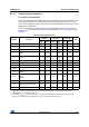
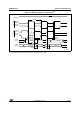
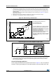
Figure 27. I
2
S slave timing diagram (Philips protocol)
(1)
1. Measurement points are done at 0.5 V
DD
level and with external C
L
= 30 pF.
2. LSB transmit/receive of the previously transmitted byte. No LSB transmit/receive is sent before the first
byte.
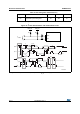
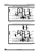
Figure 28. I
2
S master timing diagram (Philips protocol)
(1)
1. Measurement points are done at 0.5 V
DD
level and with external C
L
= 30 pF.
2. LSB transmit/receive of the previously transmitted byte. No LSB transmit/receive is sent before the first
byte.
CK Input
CPOL = 0
CPOL = 1
t
c(CK)
WS input
SD
transmit
SD
receive
t
w(CKH)
t
w(CKL)
t
su(WS)
t
v(SD_ST)
t
h(SD_ST)
t
h(WS)
t
su(SD_SR)
t
h(SD_SR)
MSB receive Bitn receive LSB receive
MSB transmit Bitn transmit LSB transmit
ai14881b
LSB receive
(2)
LSB transmit
(2)
CK output
CPOL = 0
CPOL = 1
t
c(CK)
WS output
SD
receive
SD
transmit
t
w(CKH)
t
w(CKL)
t
su(SD_MR)
t
v(SD_MT)
t
h(SD_MT)
t
h(WS)
t
h(SD_MR)
MSB receive Bitn receive LSB receive
MSB transmit Bitn transmit LSB transmit
ai14884b
t
f(CK)
t
r(CK)
t
v(WS)
LSB receive
(2)
LSB transmit
(2)