
Datasheet
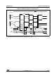
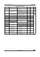
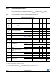

Electrical characteristics STM32F37xxx
94/131 DocID022691 Rev 4
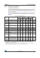
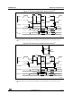
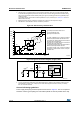
Figure 24. SPI timing diagram - slave mode and CPHA = 0
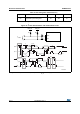
Figure 25. SPI timing diagram - slave mode and CPHA = 1
(1)
1. Measurement points are done at 0.5V
DD
level and with external C
L
= 30 pF
.
ai14134c
SCK Input
CPHA= 0
MOSI
INPUT
MISO
OUT P UT
CPHA= 0
MS B O U T
MSB IN
BI T6 OU T
LSB IN
LSB OUT
CPOL=0
CPOL=1
BIT1 IN
NSS input
t
SU(NSS)
t
c(SCK)
t
h(NSS)
t
a(SO)
t
w(SCKH)
t
w(SCKL)
t
v(SO)
t
h(SO)
t
r(SCK)
t
f(SCK)
t
dis(SO)
t
su(SI)
t
h(SI)
ai14135
SCK Input
CPHA=1
MOSI
INPUT
MISO
OUT P UT
CPHA=1
MS B O U T
MSB IN
BI T6 OU T
LSB IN
LSB OUT
CPOL=0
CPOL=1
BIT1 IN
t
SU(NSS)
t
c(SCK)
t
h(NSS)
t
a(SO)
t
w(SCLH)
t
w(SCLL)
t
v(SO)
t
h(SO)
t
r(SCL)
t
f(SCL)
t
dis(SO)
t
su(SI)
t
h(SI)
NSS input