
Datasheet

DocID022691 Rev 4 93/131
STM32F37xxx Electrical characteristics
114
SPI/I
2
S characteristics
Unless otherwise specified, the parameters given in Table 58 for SPI or in Table 59 for I
2
S
are derived from tests performed under ambient temperature, f
PCLKx
frequency and V
DD
supply voltage conditions summarized in Table 22.
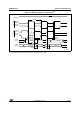
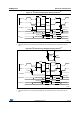
Refer to Section 6.3.14: I/O port characteristics for more details on the input/output alternate
function characteristics (NSS, SCK, MOSI, MISO for SPI and WS, CK, SD for I
2
S).
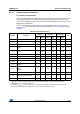
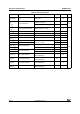
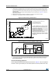
Table 58. SPI characteristics
Symbol Parameter Conditions Min Max Unit
f
SCK
1/t
c(SCK)
(1)
SPI clock frequency
Master mode - 18
MHz
Slave mode - 18
t
r(SCK)
t
f(SCK)
(1)
SPI clock rise and fall
time
Capacitive load: C = 30 pF - 8 ns
DuCy(SCK)
(1)
SPI slave input clock
duty cycle
Slave mode 30 70 %
t
su(NSS)
(1)
1. Data based on characterization results, not tested in production.
NSS setup time Slave mode 2Tpclk -
ns
t
h(NSS)
(1)
NSS hold time Slave mode 4Tpclk -
t
w(SCKH)
(1)
t
w(SCKL)
(1)
SCK high and low time
Master mode, f
PCLK
= 36 MHz,
presc = 4
Tpclk/2
- 3
Tpclk/2
+ 3
t
su(MI)
(1)
t
su(SI)
(1)
Data input setup time
Master mode 5.5 -
Slave mode 6.5 -
t
h(MI)
(1)
Data input hold time
Master mode 5 -
t
h(SI)
(1)
Slave mode 5 -
t
a(SO)
(1)(2)
2. Min time is for the minimum time to drive the output and the max time is for the maximum time to validate
the data.
Data output access time Slave mode, f
PCLK
= 24 MHz 0 4Tpclk
t
dis(SO)
(1)(3)
3. Min time is for the minimum time to invalidate the output and the max time is for the maximum time to put
the data in Hi-Z.
Data output disable time Slave mode 0 24
t
v(SO)
(1)
Data output valid time Slave mode (after enable edge) - 39
t
v(MO)
(1)
Data output valid time Master mode (after enable edge) - 3
t
h(SO)
(1)
Data output hold time
Slave mode (after enable edge) 15 -
t
h(MO)
(1)
Master mode (after enable edge) 4 -