
Datasheet

DocID022691 Rev 4 89/131
STM32F37xxx Electrical characteristics
114
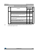
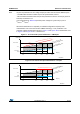
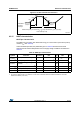
Figure 21. I/O AC characteristics definition
6.3.15 NRST characteristics
NRST pin characteristics
The NRST pin input driver uses CMOS technology. It is connected to a permanent pull-up
resistor, R
PU
(see Table 52).
Unless otherwise specified, the parameters given in Table 55 are derived from tests
performed under ambient temperature and V
DD
supply voltage conditions summarized in
Table 22.
MS32132V1
T
10%
50%
90%
10%
50%
90%
EXTERNAL
OUTPUT
ON 50 pF
Maximum frequency is achieved if (t + t (≤ 2/3)T and if the duty cycle is (45-55%)
when loaded by 50 pF
r
f
r(IO)out
t
f(IO)out
t
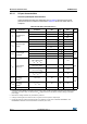
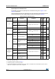
Table 55. NRST pin characteristics
Symbol Parameter Conditions Min Typ Max Unit
V
IL(NRST)
(1)
NRST Input low level voltage - - 0.3V
DD
+ 0.07
(1)
V
V
IH(NRST)
(1)
NRST Input high level voltage 0.445V
DD
+ 0.398
(1)
--
V
hys(NRST)
(1)
NRST Schmitt trigger voltage
hysteresis
-200-mV
R
PU
Weak pull-up equivalent resistor
(2)
V
IN
= V
SS
25 40 55 kΩ
V
F(NRST)
(1)
NRST Input filtered pulse - - 100 ns
V
NF(NRST)
(1)
NRST Input not filtered pulse 500 - - ns
1. Data based on design simulation only, not tested in production.
2. The pull-up is designed with a true resistance in series with a switchable PMOS. This PMOS contribution to the series
resistance is minimal (~10% order).