
Datasheet

DocID022691 Rev 4 87/131
STM32F37xxx Electrical characteristics
114
Output voltage levels
Unless otherwise specified, the parameters given in Table 53 are derived from tests
performed under ambient temperature and V
DD
supply voltage conditions summarized in
Table 22. All I/Os are CMOS and TTL compliant (FT, TTa or TC unless otherwise specified).
Note: I/O pins are powered from V
DD
voltage except pins which can be used as SDADC inputs:
- The PB2, PB10 and PE7 to PE15 I/O pins are powered from V
DDSD12
.
- PB14 to PB15 and PD8 to PD15 I/O pins are powered from V
DDSD3
. All I/O pin ground is
internally connected to V
SS
.
V
DD
mentioned in the Table 53 represents power voltage for a given I/O pin (V
DD
or
V
DDSD12
or V
DDSD3
).
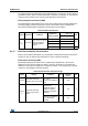
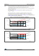
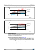
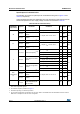
Table 53. Output voltage characteristics
(1)
1. VDDSD12 is the external power supply for PB2, PB10, and PE7 to PE15 I/O pins (the I/O ground pin is
internally connected to VSS). VDDSD3 is the external power supply for PB14 to PB15 and PD8 to PD15
I/O pins (the I/O ground pin is internally connected to VSS). For those pins all V
DD
supply references in this
table are related to their given VDDSDx power supply.
Symbol Parameter Conditions Min Max Unit
V
OL
(2)
2. The I
IO
current sunk by the device must always respect the absolute maximum rating specified in Table 20
and the sum of I
IO
(I/O ports and control pins) must not exceed I
VSS
.
Output low level voltage for an I/O pin CMOS port
(3)
I
IO
= +8 mA
2.7 V < V
DD
< 3.6 V
3. TTL and CMOS outputs are compatible with JEDEC standards JESD36 and JESD52.
-0.4
V
V
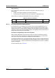
OH
(4)
4. The I
IO
current sourced by the device must always respect the absolute maximum rating specified in
Table 20 and the sum of I
IO
(I/O ports and control pins) must not exceed I
VDD
.
Output high level voltage for an I/O pin V
DD
–0.4 -
V
OL
(2)
Output low level voltage for an I/O pin TTL port
(3)
I
IO
= +8 mA
2.7 V < V
DD
< 3.6 V
-0.4
V
OH
(4)
Output high level voltage for an I/O pin 2.4 -
V
OL
(2)(5)
5. Data based on design simulation.
Output low level voltage for an I/O pin
I
IO
= +20 mA
2.7 V < V
DD
< 3.6 V
-1.3
V
OH
(4)(5)
Output high level voltage for an I/O pin V
DD
–1.3 -
V
OL
(2)(5)
Output low level voltage for an I/O pin
I
IO
= +6 mA
2 V < V
DD
< 2.7 V
-0.4
V
OH
(4)(5)
Output high level voltage for an I/O pin V
DD
–0.4 -
V
OLFM+
(2)
Output low level voltage for a FTf I/O pins
in FM+ mode
I
IO
= +20 mA
2.7 V < V
DD
< 3.6 V
-0.4