
Datasheet

Electrical characteristics STM32F37xxx
86/131 DocID022691 Rev 4
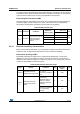
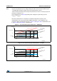
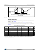
Figure 19. Five volt tolerant (FT and FTf) I/O input characteristics - CMOS port
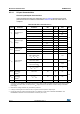
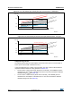
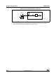
Figure 20. Five volt tolerant (FT and FTf) I/O input characteristics - TTL port
Output driving current
The GPIOs (general purpose input/outputs) can sink or source up to ± 8 mA, and sink or
source up to ± 20 mA (with a relaxed V
OL/
V
OH
).
In the user application, the number of I/O pins which can drive current must be limited to
respect the absolute maximum rating specified in Section 6.2:
• The sum of the currents sourced by all the I/Os on all VDD_x and VDDSDx, plus the
maximum Run consumption of the MCU sourced on V
DD
cannot exceed the absolute
maximum rating
ΣI
VDD
(see Table 20).
• The sum of the currents sunk by all the I/Os on all VSS_x and VSSSD, plus the
maximum Run consumption of the MCU sunk on V
SS
cannot exceed the absolute
maximum rating
ΣI
VSS
(see Table 20).
V
DD
(V)
2.0
0.5
V
IL
/V
IH
(V)
2.0 3.6
1.0
2.7
Area not determined
MS30257V3
V
ILmax
= 0.475V
DD
-0.2
V
IHmin
= 0.5V
DD
+0.2
Based on design simulations
Based on design simulations
CMOS standard requirements V
IHmin
= 0.7V
DD
CMOS standard requirements V
ILmax
= 0.3V
DD
V
DD
(V)
2.0
0.5
V
IL
/V
IH
(V)
2.0 3.6
1.0
2.7
Area not determined
MS30258V4
V
ILmax
= 0.475V
DD
-0.2
V
IHmin
= 0.5V
DD
+0.2
Based on design simulations
Based on design simulations
TTL standard requirements V
IHmin
= 2 V
TTL standard requirements V
ILmax
= 0.8 V
0.8