
Datasheet

DocID022691 Rev 4 85/131
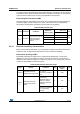
STM32F37xxx Electrical characteristics
114
Note: I/O pins are powered from V
DD
voltage except pins which can be used as SDADC inputs:
- The PB2, PB10 and PE7 to PE15 I/O pins are powered from V
DDSD12
.
- PB14 to PB15 and PD8 to PD15 I/O pins are powered from V
DDSD3
. All I/O pin ground is
internally connected to V
SS
.
V
DD
mentioned in the Table 52 represents power voltage for a given I/O pin (V
DD
or
V
DDSD12
or V
DDSD3
).
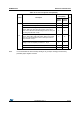
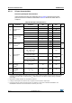
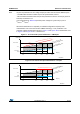
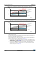
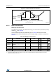
All I/Os are CMOS and TTL compliant (no software configuration required). Their
characteristics cover more than the strict CMOS-technology or TTL parameters. The
coverage of these requirements is shown in Figure 17 and Figure 18 for standard I/Os, and
in Figure 19 and Figure 20 for 5 V tolerant I/Os.
Figure 17. TC and TTa I/O input characteristics - CMOS port
Figure 18. TC and TTa I/O input characteristics - TTL port
MS30255V2
V
DD
(V)
V
IHmin
2.0
V
ILmax
0.7
V
IL
/V
IH
(V)
1.3
2.0 3.6
V
ILmax
= 0.3V
DD
+0.07
0.6
2.7 3.0 3.3
CMOS standard requirements V
ILmax
= 0.3V
DD
V
IHmin
= 0.445V
DD
+0.398
Area not determined
Tested in production
Tested in production
Based on design simulations
Based on design simulations
CMOS standard requirements V
IHmin
= 0.7 V
DD
V
DD
(V)
V
IHmin
2.0
V
ILmax
0.7
V
IL
/V
IH
(V)
1.3
2.0 3.6
V
ILmax
= 0.3V
DD
+
0.07
0.8
2.7 3.0 3.3
V
IHmin
= 0.445V
DD
+0.398
Area not determined
Based on design simulations
Based on design simulations
MS30256V4
TTL standard requirements V
IHmin
= 2 V
TTL standard requirements V
ILmax
= 0.8 V